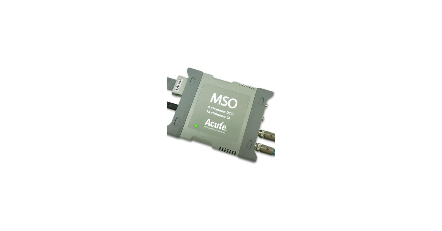
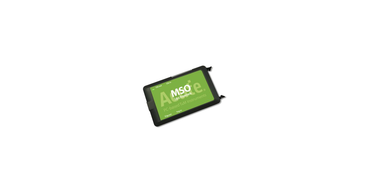
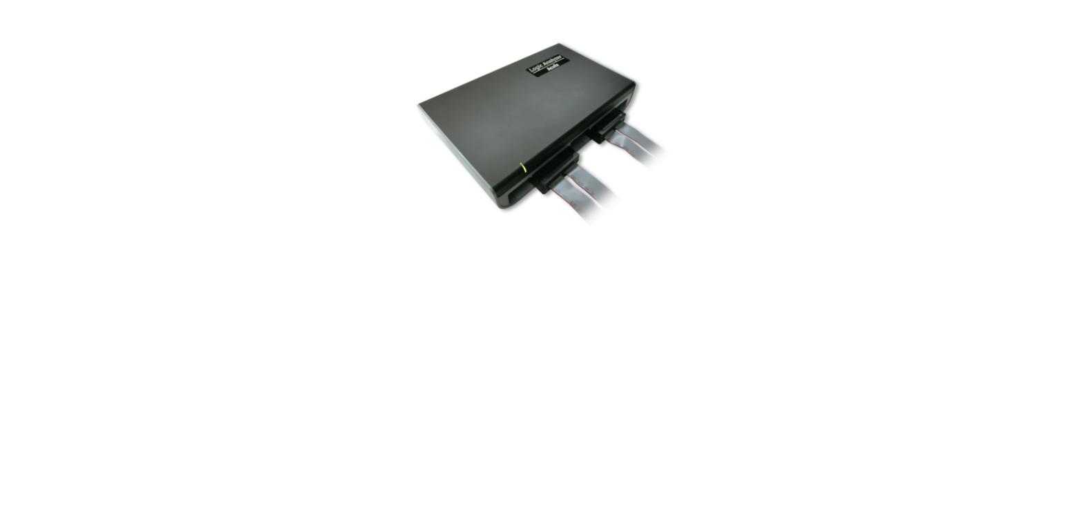
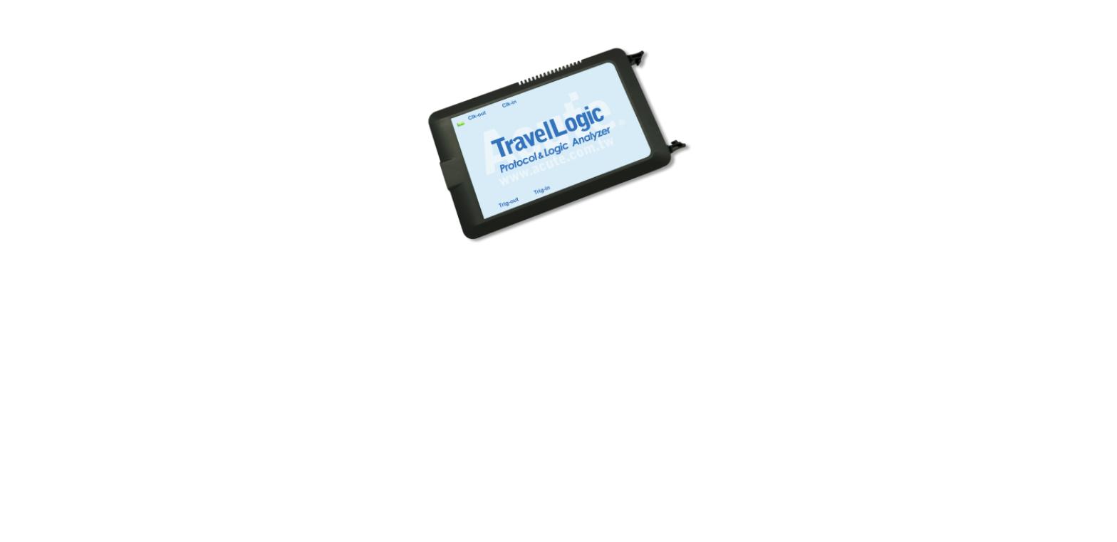
The MSO3124V adds electrical validation to the MSO3124H spec — protocol-aware triggering and decode (I2C, I3C, SPI, UART and more) directly on the analog waveform, not just the digital channels.
Highlights
4 analog / 16 digital channels, 200MHz bandwidth, 1GS/s
The MSO2216B doubles the MSO2116 pair’s memory to 8Gb and adds eSPI, SVI3 and SVID support — useful when a longer capture window or those specific protocols are part of the debug.
The MSO2116E combines 16 analog and 16 digital channels behind one trigger — a compact way to see a control edge and its analog consequence in the same capture without cascading two separate instruments.
Highlights
16 analog / 16 digital channels, 40MHz bandwidth
200MS/s sample rate, 4Gb total memory
2GHz timing / 200MHz state analysis on the digital side
The LA4136E is LA4000’s full 136-channel configuration — the widest logic analyzer in Acute’s standard line, for backplane and multi-drop bus debug where channel count is the limiting factor.
The LA4068E is LA4000’s 68-channel entry point — the same 4GHz timing engine and 32Gb of memory as the wider 136-channel units, sized for boards that need more than TravelLogic’s 34 channels but not a full 136-wide backplane.
The TL4134E carries the same 34-channel, 2GHz, 4Gb spec as the TL4134B in an alternate interface variant — same capture performance, different connector/interface fit.
The TL4234B doubles the TL4134B’s memory to 8Gb and adds explicit eSPI and SVID support — the pick when a longer capture window or those specific protocols matter more than saving on memory.
The TL4134B is TravelLogic’s standard 34-channel unit: 2GHz timing analysis and 4Gb of capture memory, enough headroom for a real board bring-up session rather than a short triggered snapshot.
Highlights
34 channels, 2GHz timing / 250MHz state analysis
4Gb total memory, 512Mb max record length
Full protocol decode/trigger library (90+ bus decodes)
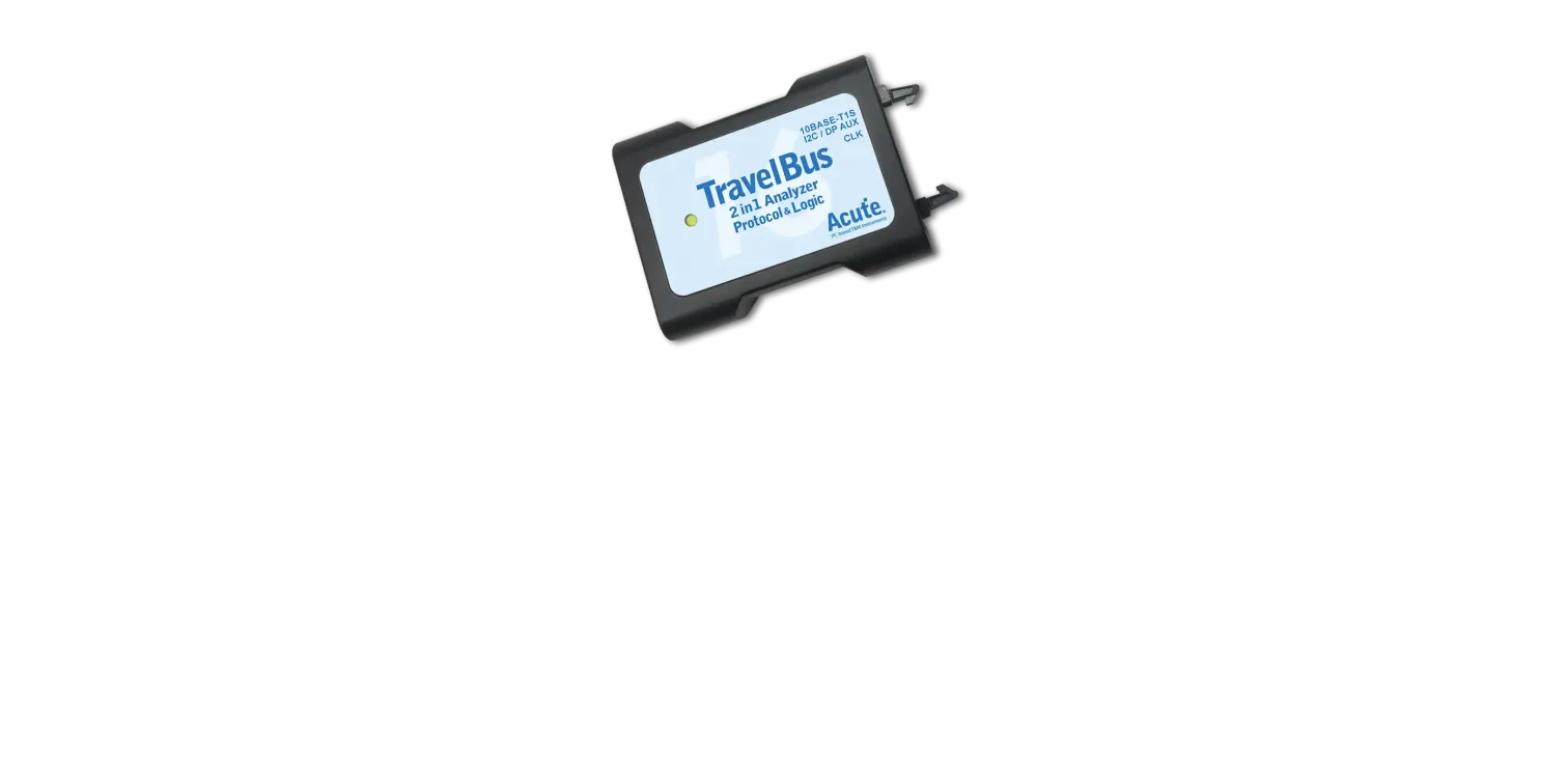
The TB3016F matches the TB3016E’s 19-channel, 800MHz spec in an alternate interface/connector configuration — pick whichever fits your existing fixture without changing capture performance.
Highlights
19 channels, 800MHz timing / 200MHz state analysis
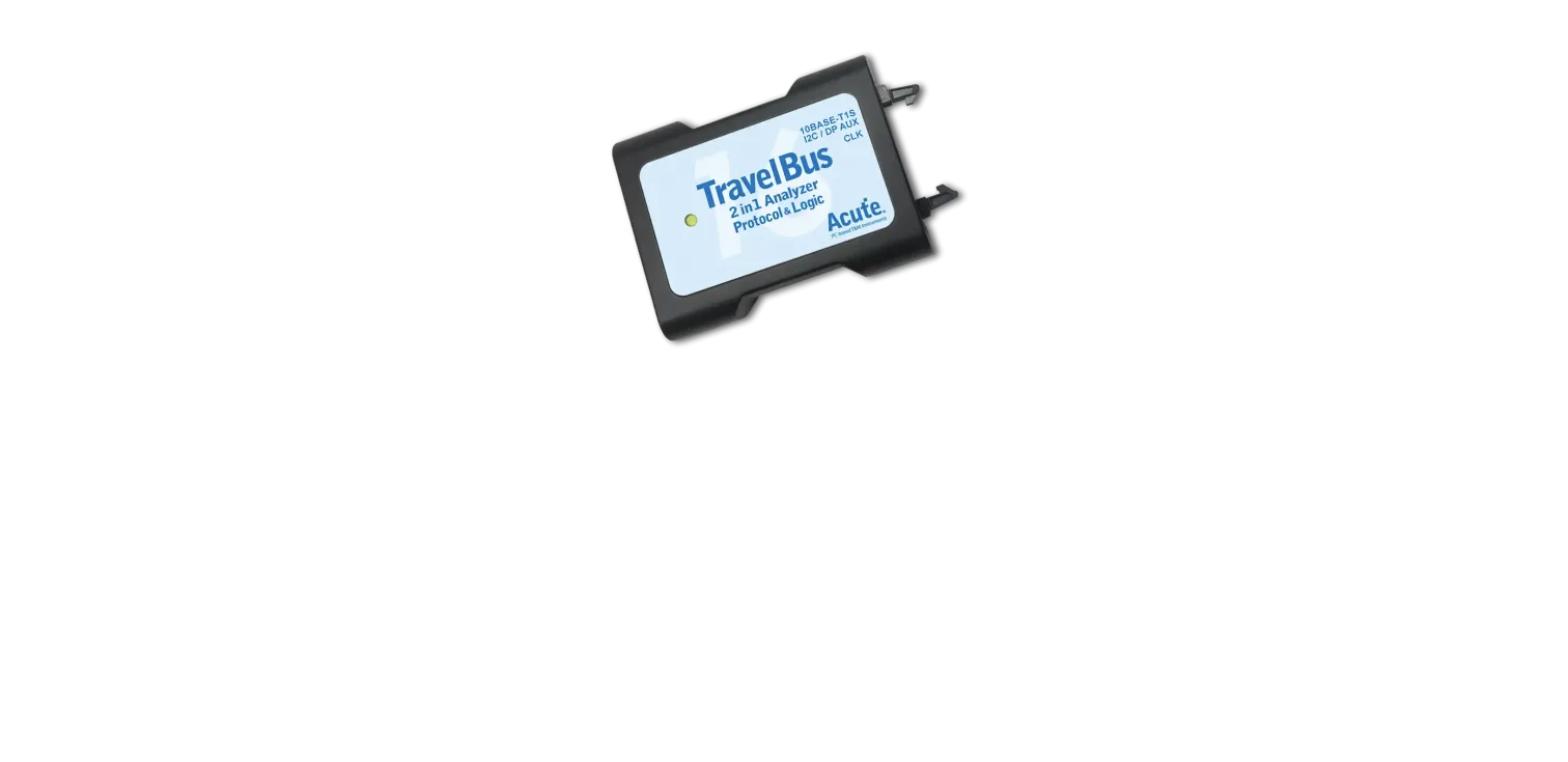
The TB3016E is TravelBus’s standard 19-channel configuration, adding DP_Aux differential decode to the same 800MHz timing engine as the rest of the line — a compact entry point into Acute’s protocol + logic analysis platform.
Highlights
19 channels, 800MHz timing / 200MHz state analysis
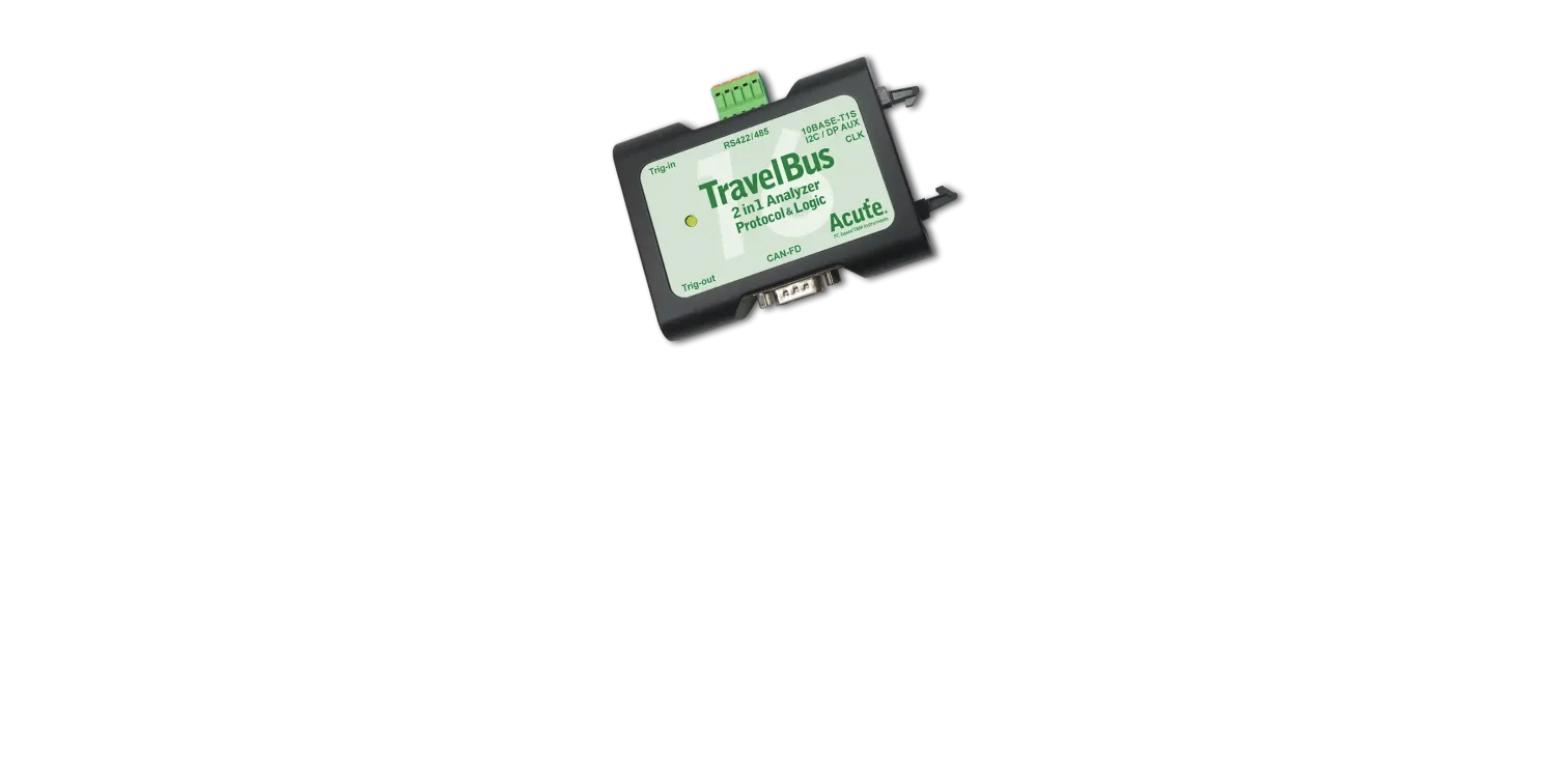
The TB3016B is the top TravelBus configuration, pairing 25 general-purpose channels with built-in differential decode for CAN2.0/CAN-FD, RS422/RS485 and DP_Aux — useful when a board mixes single-ended debug signals with a differential bus on the same header.
Highlights
25 channels, 800MHz timing / 200MHz state analysis
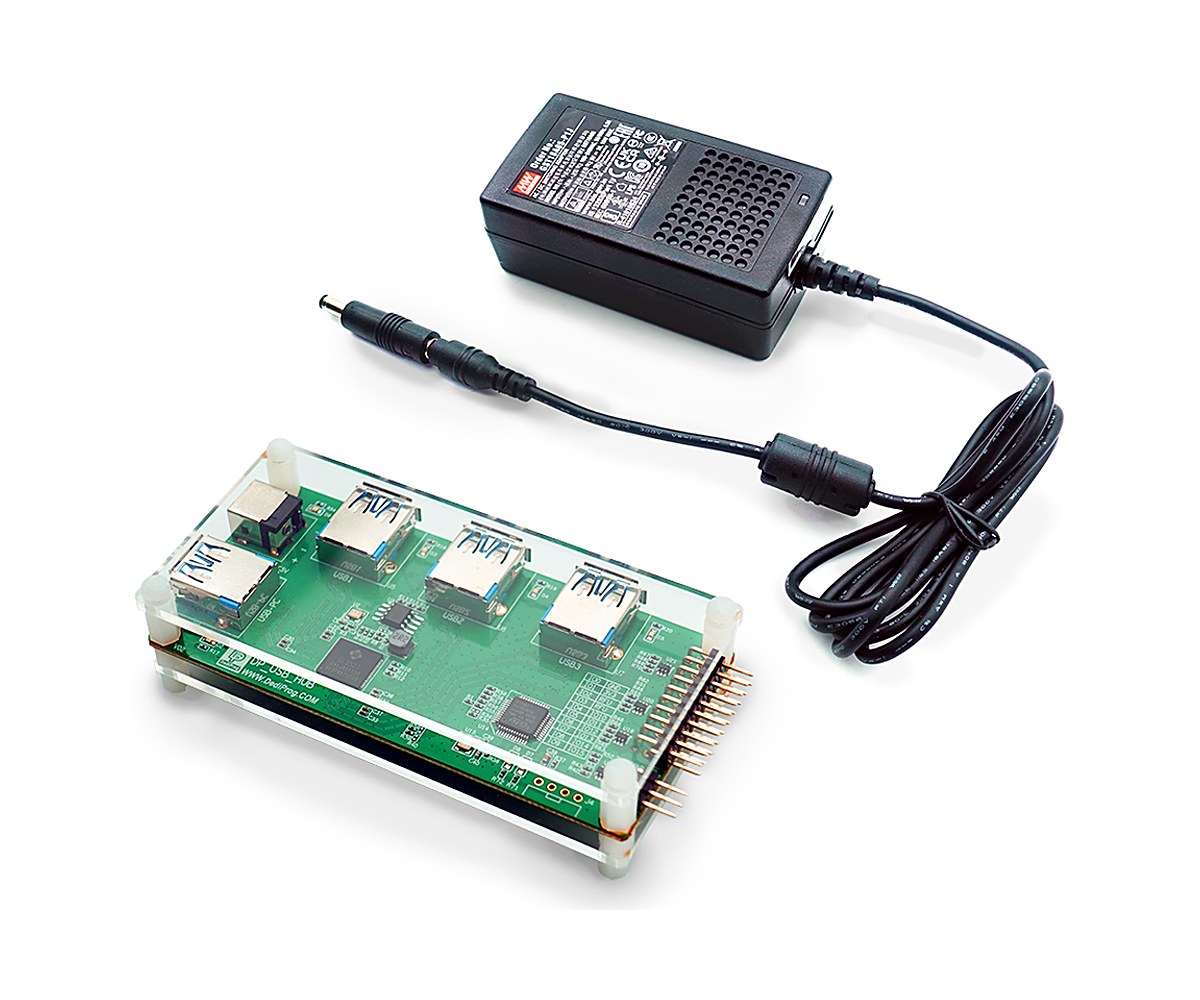
More than a standard USB hub – allows engineers to control and monitor the power supply of its three USB ports via commands, useful for remote power control in IC programming tasks.
Specifications
3 USB ports with individual power control
Includes power cord
Key Specifications
Spec
Value
Ports
3x USB, individually power-controlled
Function
Remote power control/monitoring per port for IC programming automation
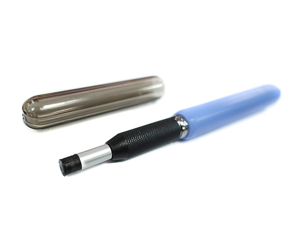
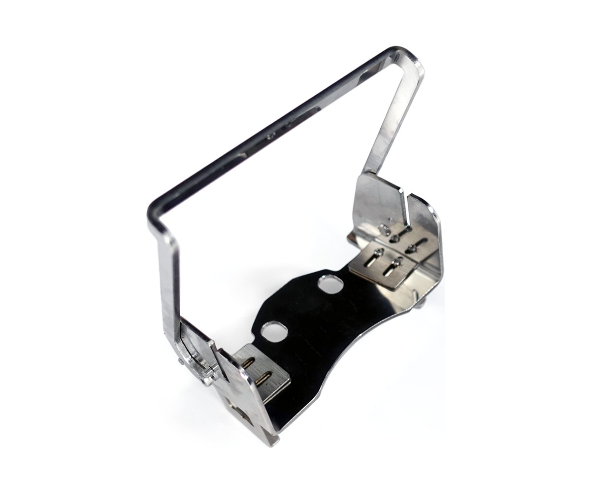
Designed for cleaning contact surfaces of Pressure Conductive Silicon Rubber (PCR); removes oxide buildup for stable, reliable electrical connections and extends PCR service life.
Interchangeable Plug Power Adapter – ME-AD-010-005-020-002-A
Power adapter for SF600Plus, SF600Plus-G2, EM100Pro-G2/G3, and NuProg-E2; recommended for EM100Pro-G2/G3 if USB power is insufficient and causes unstable signaling.
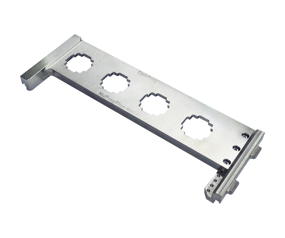
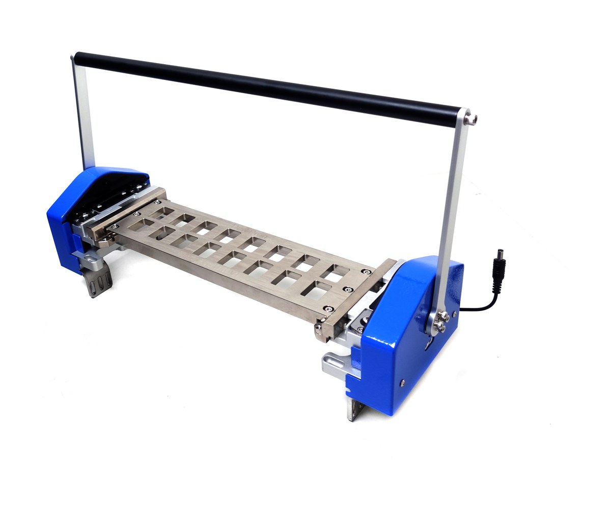
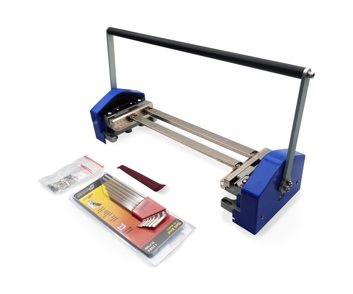
For use with the NuProgPlus Hand Press Fixture only. Designed for the DediProg M4545 programming socket; maximizes programming efficiency for high pin count devices.
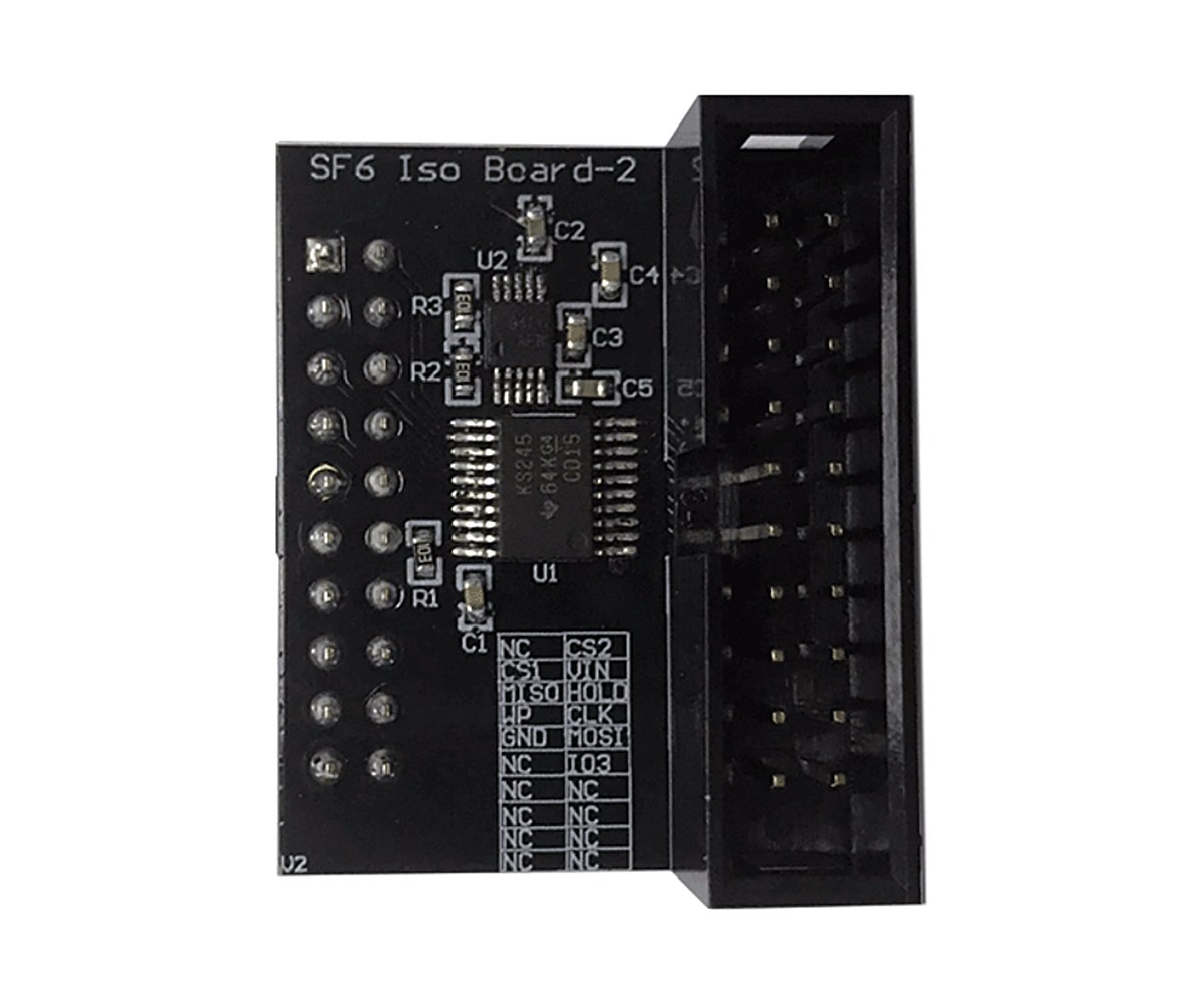
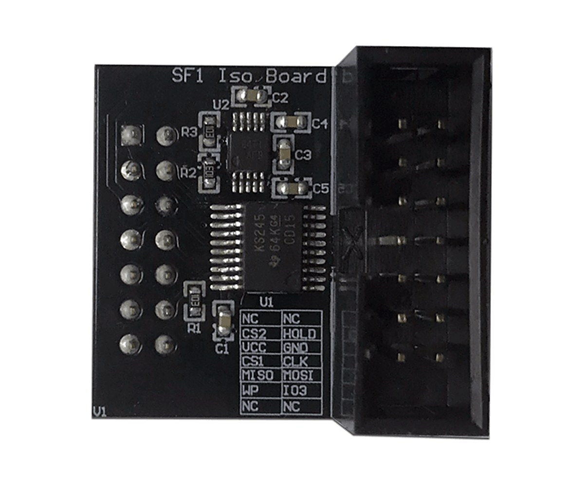
Isolation board that reduces cable interference to motherboard boot performance when SF100 is attached; installed between cable and SF100 if interference occurs.
Specifications
Compatible with SF100 programmer
Key Specifications
Spec
Value
Purpose
Reduces cable interference to motherboard boot performance during attachment
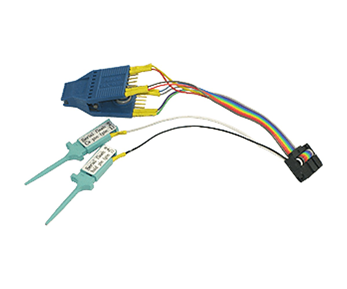
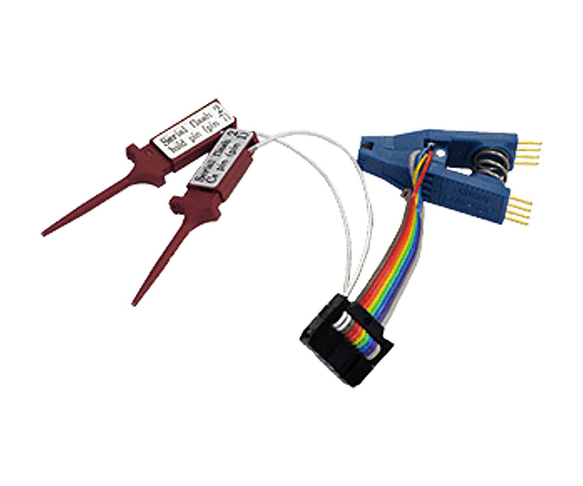
Connects dual backup boot flash tools to two main serial flash chips on board; one SO16W test clip plus two individual clips for chip-select/hold pins.
BBF Testclip For Dual Flash (SO8W 207mil) – BBF-2TC-8
Connects the Dual Backup Boot Flash Tool to two main serial flash chips on a board without connectors; one SO8 test clip for the first flash plus two individual clips for chip-select/hold pins on the second.
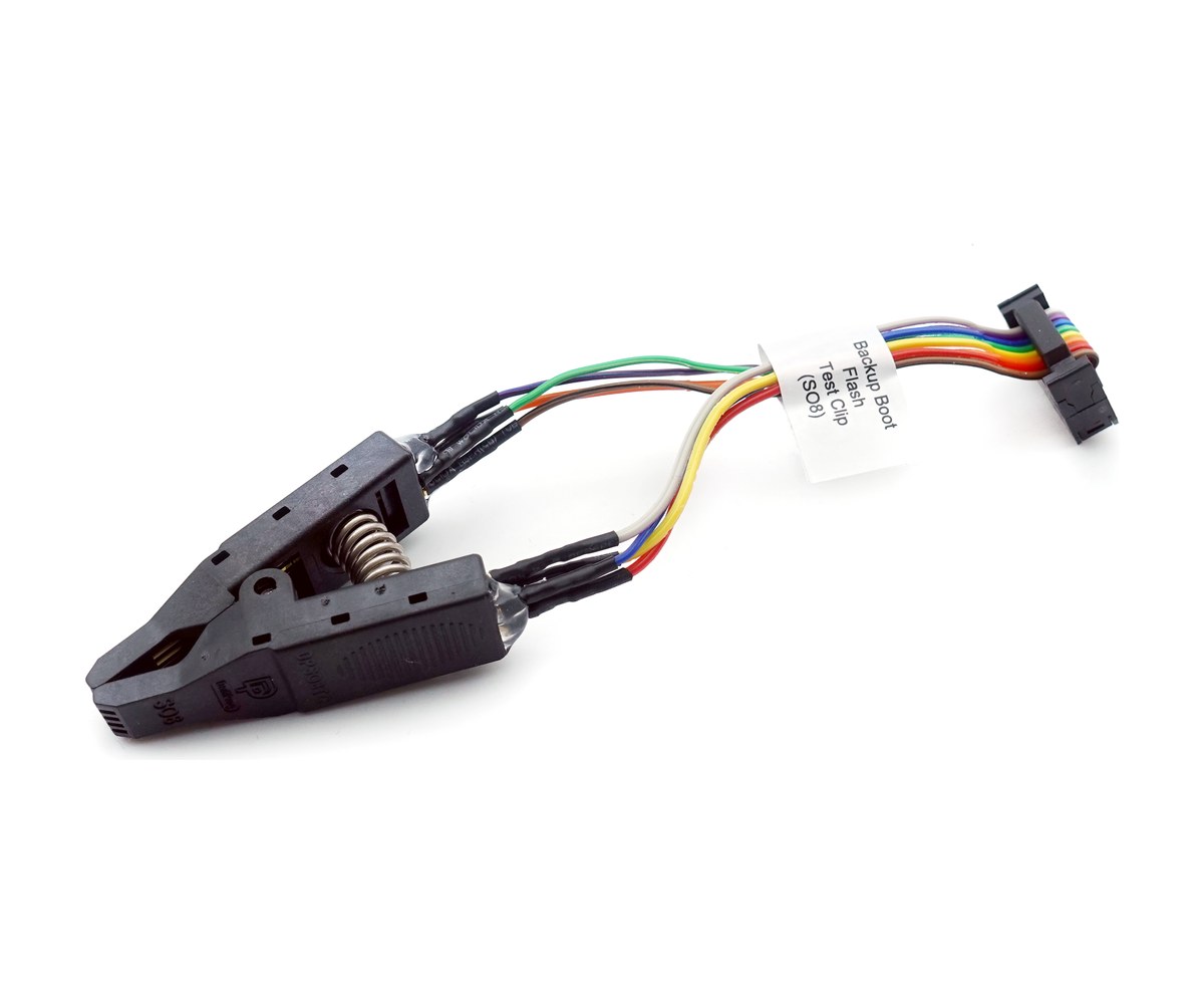
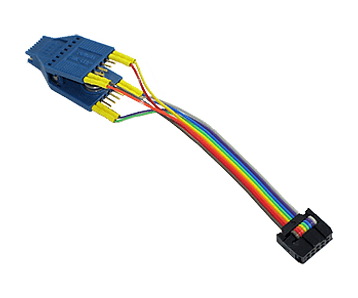
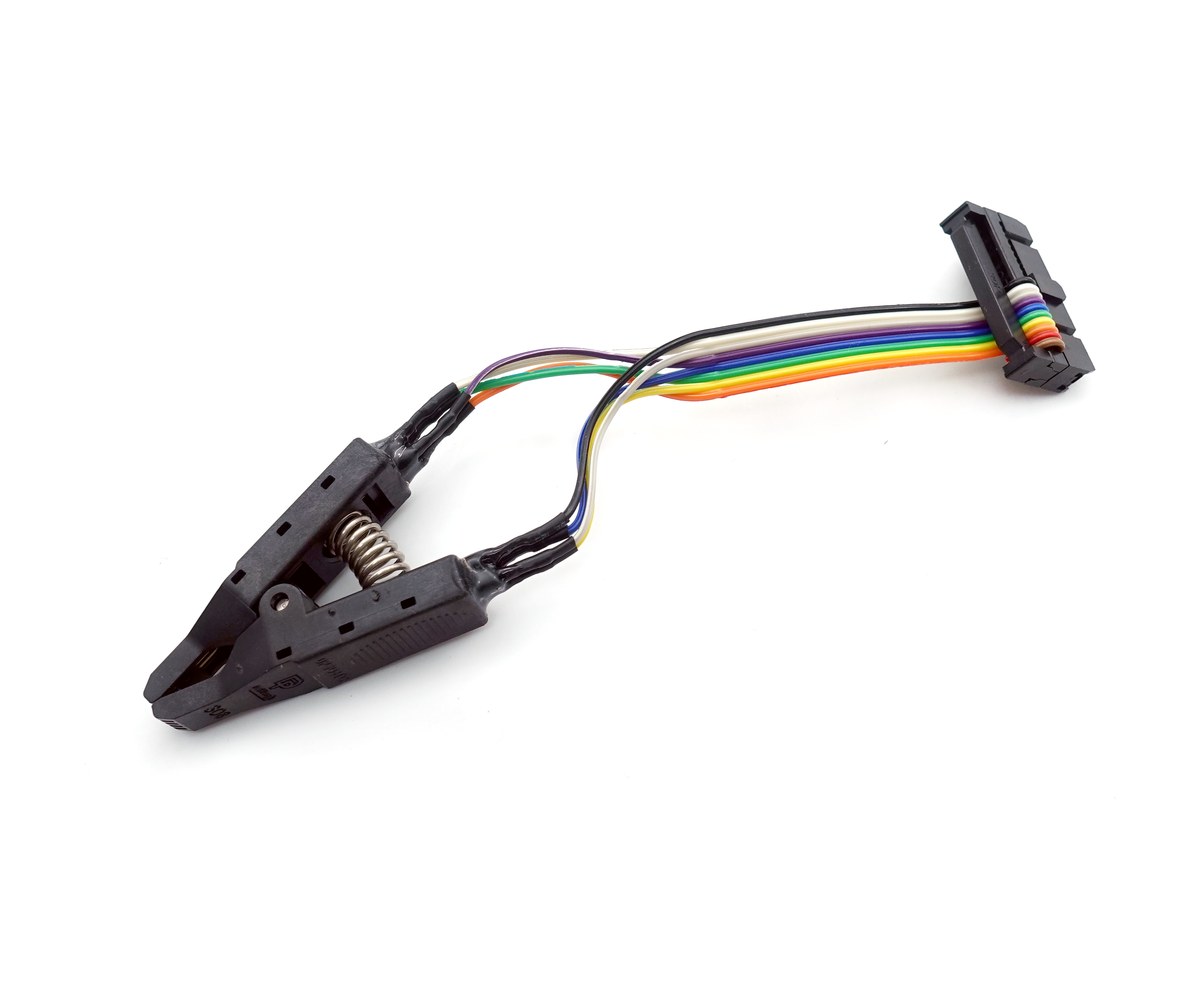
Connects the Backup Boot Flash Tool to serial flash soldered on boards for automatic operation without a connector; used for BIOS development and desktop/notebook repair.
Specifications
SO8N (150mil) and SO8W (207mil) compatible
No hardware modification needed
Key Specifications
Spec
Value
Package
SO8N (150mil) / SO8W (200mil)
Use Case
Connects Backup Boot Flash Tool to main serial flash, no hardware mod
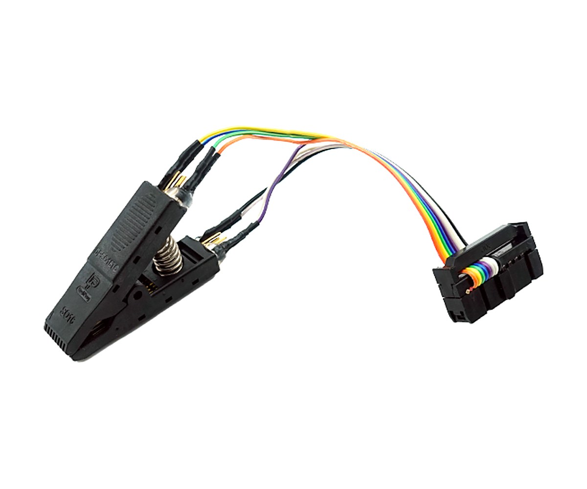
Connects backup boot flash tools to main serial flash for automatic backup flash operations without a connector; used with BIOS development and repair.
Specifications
SO16W, 300mil pitch
Key Specifications
Spec
Value
Package
SO16W (300mil)
Use Case
Connects Backup Boot Flash Tool to main serial flash, no hardware mod
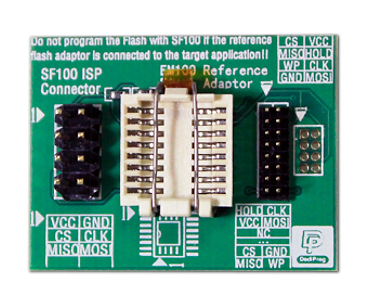
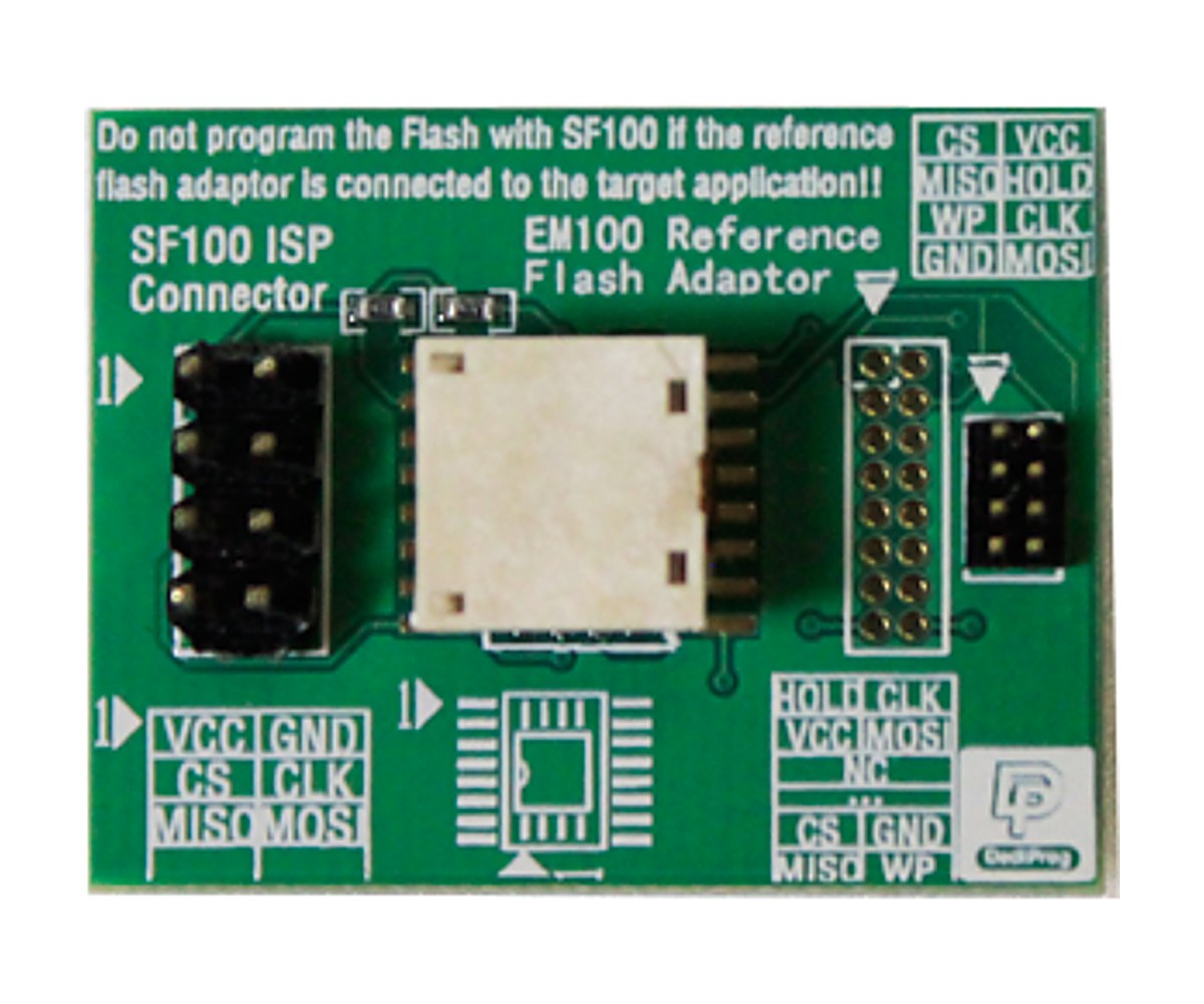
Connects EM100/EM100Pro and SF600/SF600Plus programmers to serial flash soldered on boards, letting the application controller work automatically without a connector.
Specifications
SO8N (150mil) and SO8W (200mil) compatible
2×10 connector
No hardware modification needed for most applications
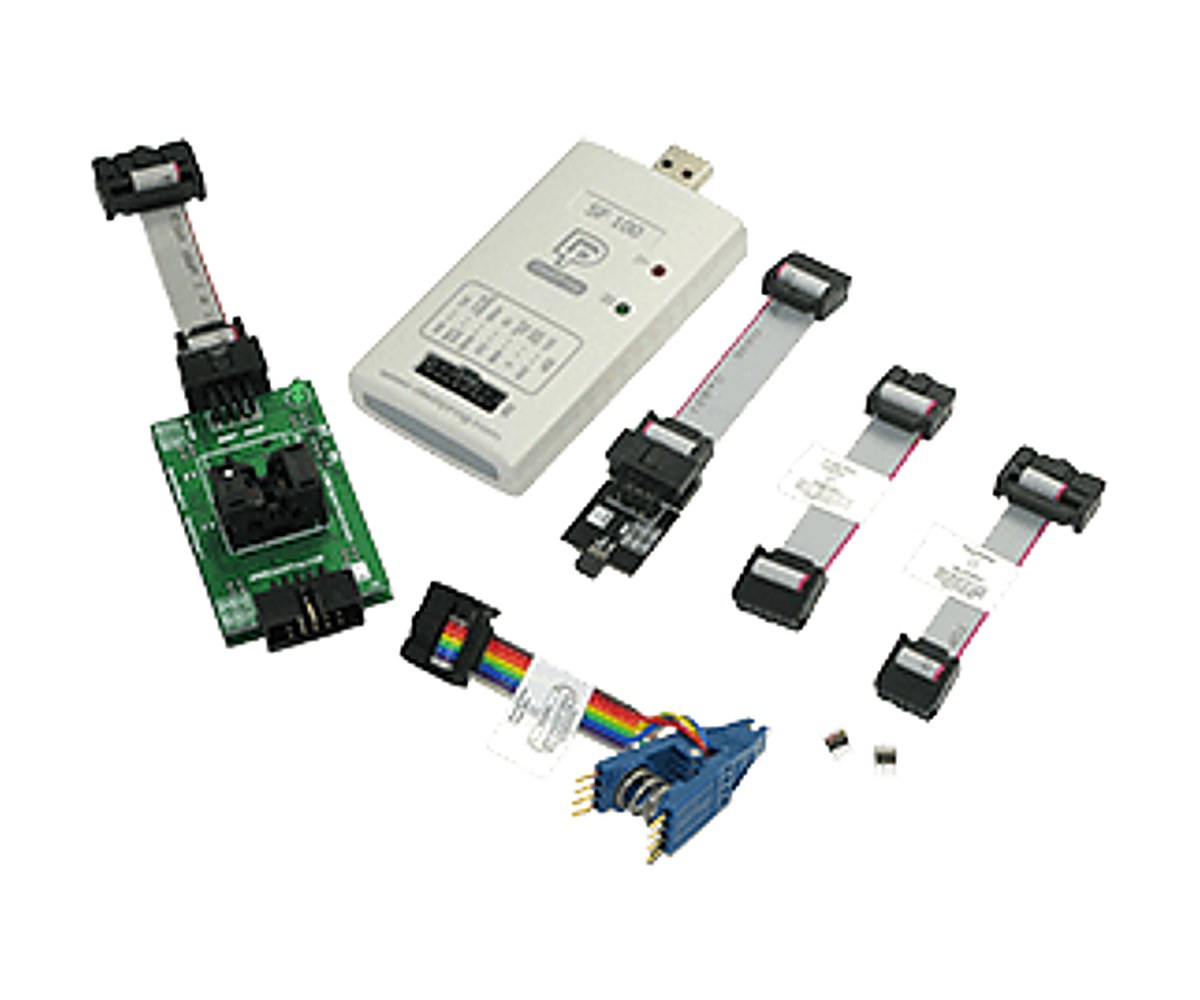
The SBK09 lets a board that uses an SO8N (150mil) SPI flash boot from a backup chip instead of the soldered one. The backup sits in DediProg’s BBF-8N Backup Boot Flash module. When it is connected, the onboard flash is disabled automatically, with no need to remove it. The module is transparent to the application, and most boards need no hardware change.
The SF100 programmer in the kit writes new images to the backup flash, so you can try a new build or go back to a known-good one without touching a soldering iron. The kit is also often used to boot a PC or board whose BIOS update failed, and then repair the corrupted BIOS with the usual flash utility tools.
Highlights
Serial flash emulator, transparent to the application
Disables the onboard serial flash automatically, with no need to remove it
No hardware change needed on most boards
Image download at 1Mbit/s, read at 2Mbit/s
USB interface with signal conflict protection
Two Ways to Connect
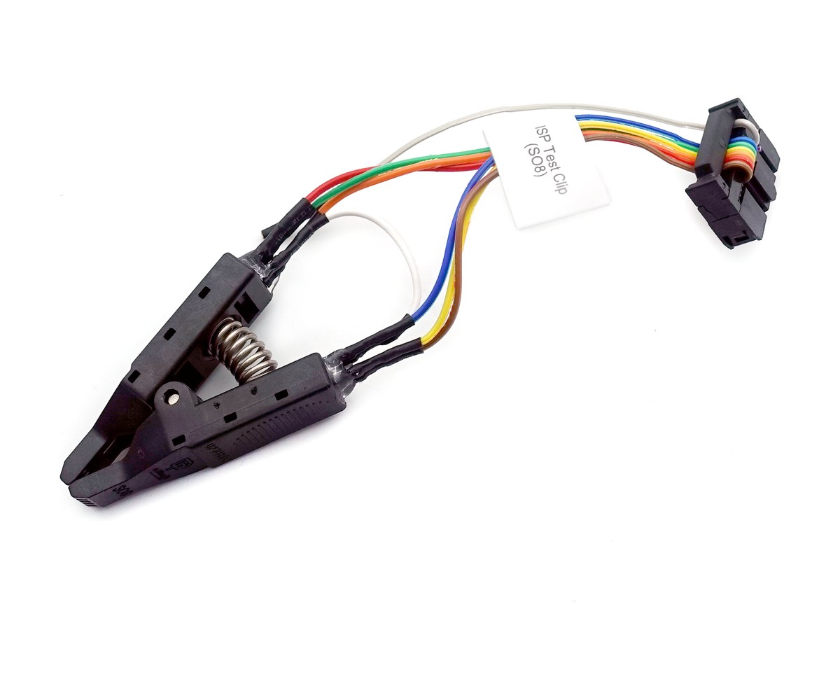
The SO8 test clip on the soldered flash
A 2.54mm 2×5 BBF connector, if the board was designed with one
Typical Uses
Booting a failing PC or board and repairing a corrupted BIOS
Trying new firmware builds without reflashing the soldered chip
Key Specifications
Spec
Value
Backup flash module
BBF-8N, SO8N (150mil) socket
Programmer
SF100, USB
Supported ICs
3.3V and 2.5V only
Speed
1Mbit/s download, 2Mbit/s read
Connection
SO8 test clip, or 2.54mm 2×5 BBF connector
Board requirement
HOLD pin pulled high through a resistor
For offline programming only, a socket adaptor is the better choice than a BBF kit.
In the Box
SF100 programmer with USB cable and SF100 ISP cable (ISP1-CB)
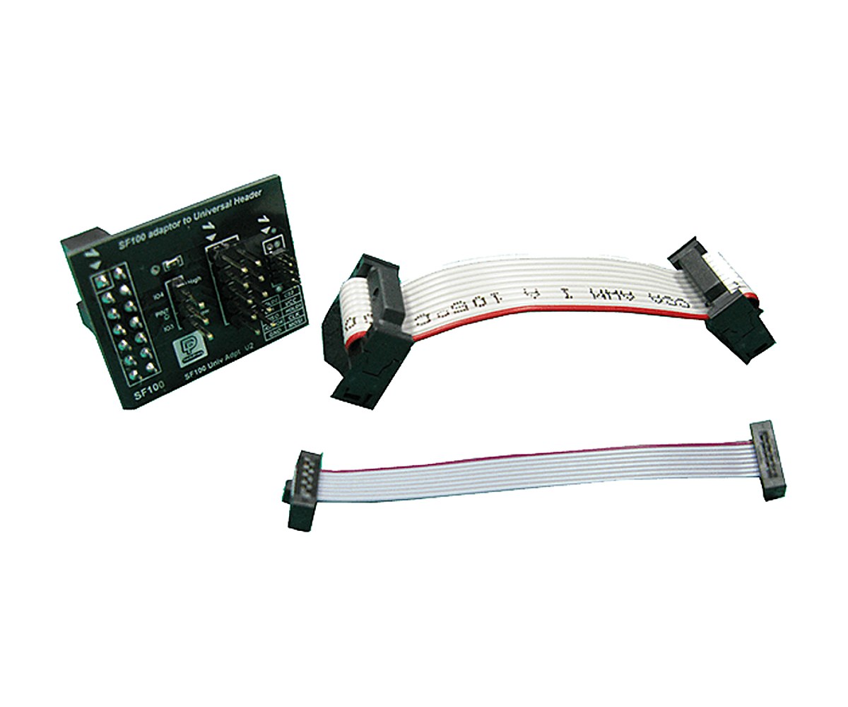
Universal adaptor (ISP-UADP-127) with BBF cable and 1.27mm 2×4 cable
CD-ROM with software, specifications and user manual
BBF-8N module with SO8N socket
BBF cable with 2.54mm 2×5 female header
SO8 connection adaptor (BBF-CON-8) with four 1.27mm 2×4 SMT headers and a 1.27mm 2×4 cable
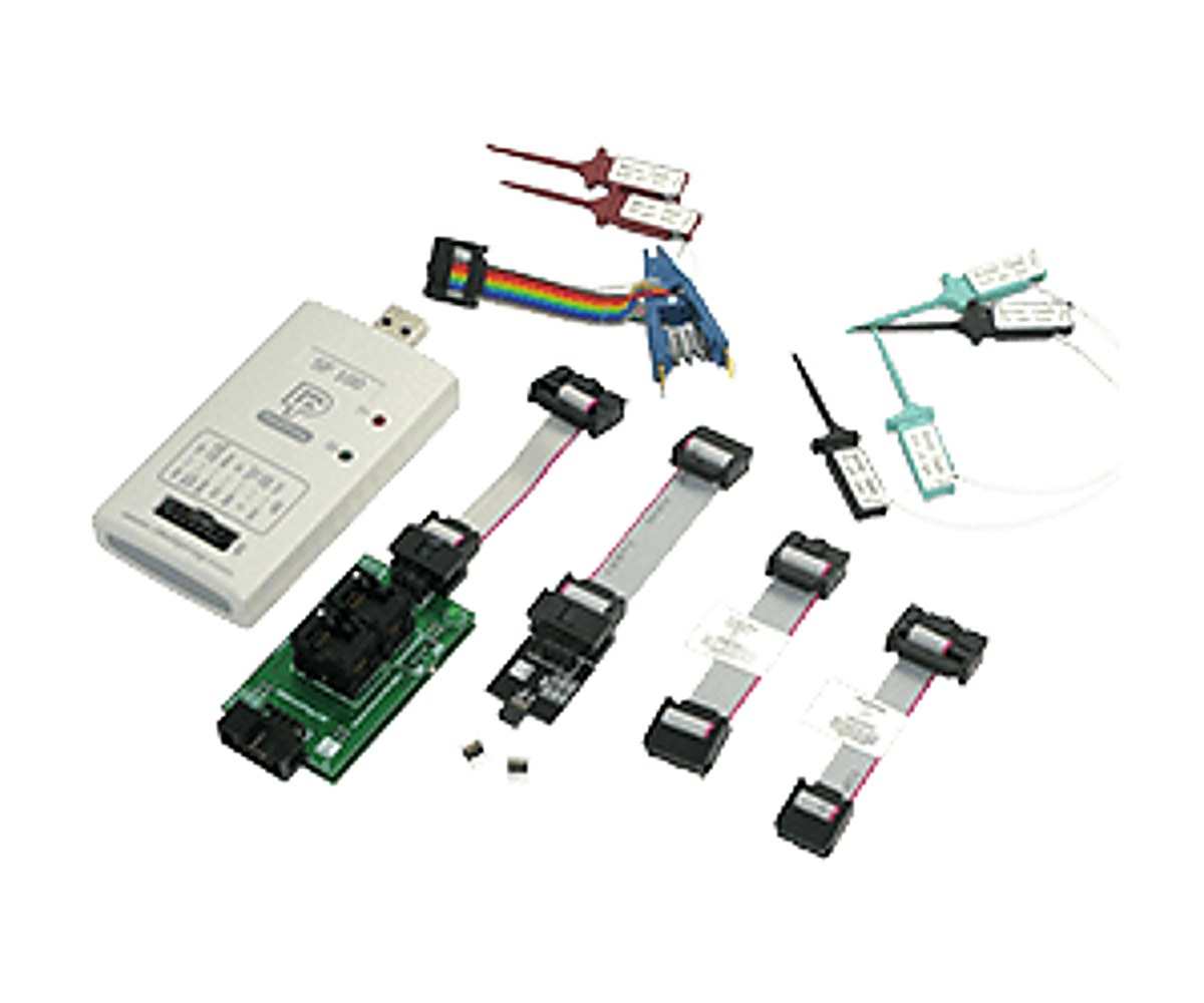
The SBK05 is for boards that carry two SO8W (207mil) SPI flash devices. Both backup chips sit in DediProg’s BBF-D8W Backup Boot Flash module. When it is connected, the board boots from them and the two onboard flash chips are disabled automatically, with no need to remove them. The module is transparent to the application, and most boards need no hardware change.
The SF100 programmer in the kit writes new images to the backup flash chips, so you can try a new build or go back to a known-good one without touching a soldering iron. The kit is also often used to boot a PC or board whose BIOS update failed, and then repair the corrupted BIOS with the usual flash utility tools.
Highlights
Dual serial flash emulator, transparent to the application
Disables the onboard serial flash automatically, with no need to remove them
No hardware change needed on most boards
Image download at 1Mbit/s, read at 2Mbit/s
USB interface with signal conflict protection
Three Ways to Connect
The dual BBF test clip on the two soldered flash chips
Two SMT 1.27mm headers soldered in place of the flash footprints, with the dual-header cable adaptor
A 2.54mm 2×5 BBF connector, if the board was designed with one
Typical Uses
Boards with two SPI flash devices on one SPI bus
Booting a failing PC or board and repairing a corrupted BIOS
Trying new firmware builds without reflashing the soldered chip
Key Specifications
Spec
Value
Backup flash module
BBF-D8W, two SO8W (207mil) sockets
Programmer
SF100, USB
Supported ICs
3.3V and 2.5V only
Speed
1Mbit/s download, 2Mbit/s read
Connection
Dual test clip, two SMT 1.27mm headers, or 2.54mm 2×5 BBF connector
Board requirement
Pull-up resistor between the HOLD pin and Vcc when the onboard flash stays on the board. The two flash devices must share one SPI bus, with separate chip selects
For offline programming only, a socket adaptor is the better choice than a BBF kit.
In the Box
SF100 programmer with USB cable and SF100 ISP cable (ISP1-CB)
Universal adaptor (ISP-UADP-127) with BBF cable and 1.27mm 2×4 cable
CD-ROM with software, specifications and user manual
BBF-D8W module with two SO8W sockets
BBF cable with 2.54mm 2×5 female header
SO8 connection adaptor (BBF-CON-8) with four 1.27mm 2×4 SMT headers
Two BBF grabber cables for dual SPI
1.27mm 2×4 cable with female header
Dual BBF test clip (BBF-2TC-8), SO8N and SO8W compatible
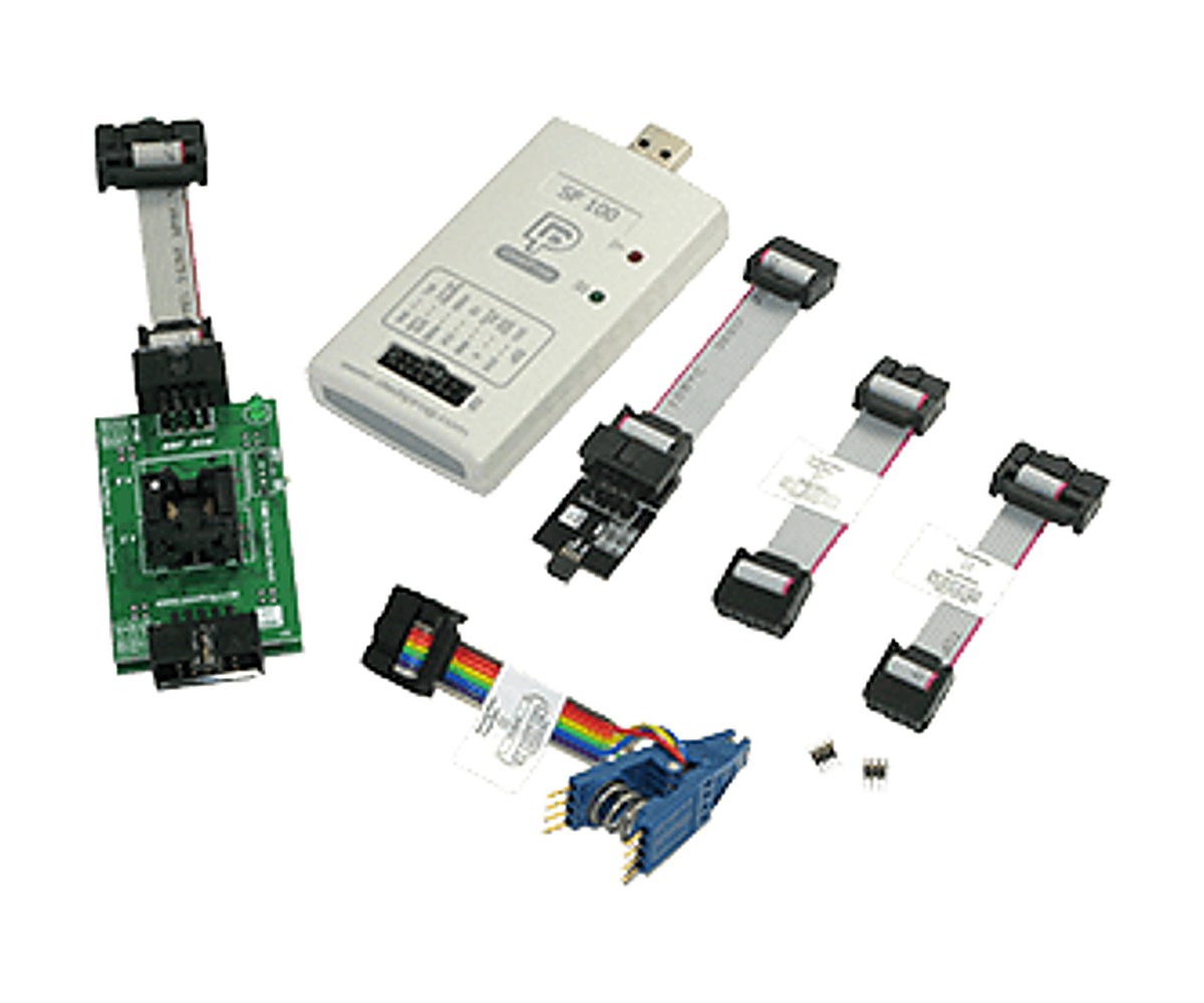
The SBK01 lets a board that uses an SO8W (207mil) SPI flash boot from a backup chip instead of the soldered one. The backup sits in DediProg’s BBF-8W Backup Boot Flash module. When it is connected, the onboard flash is disabled automatically, with no need to remove it. The module is transparent to the application, and most boards need no hardware change.
The SF100 programmer in the kit writes new images to the backup flash, so you can try a new build or go back to a known-good one without touching a soldering iron. The kit is also often used to boot a PC or board whose BIOS update failed, and then repair the corrupted BIOS with the usual flash utility tools.
Highlights
Serial flash emulator, transparent to the application
Disables the onboard serial flash automatically, with no need to remove it
No hardware change needed on most boards
Image download at 1Mbit/s, read at 2Mbit/s
USB interface with signal conflict protection
Three Ways to Connect
The BBF test clip on the soldered flash
An SMT 1.27mm header soldered in place of the flash footprint, for a steadier connection
A 2.54mm 2×5 BBF connector, if the board was designed with one
Typical Uses
Booting a failing PC or board and repairing a corrupted BIOS
Trying new firmware builds without reflashing the soldered chip
Key Specifications
Spec
Value
Backup flash module
BBF-8W, SO8W (207mil) socket
Programmer
SF100, USB
Supported ICs
3.3V and 2.5V only
Speed
1Mbit/s download, 2Mbit/s read
Connection
Test clip, SMT 1.27mm header, or 2.54mm 2×5 BBF connector
Board requirement
Pull-up resistor between the HOLD pin and Vcc when the onboard flash stays on the board
For offline programming only, a socket adaptor is the better choice than a BBF kit.
In the Box
SF100 programmer with USB cable and SF100 ISP cable (ISP1-CB)
Universal adaptor (ISP-UADP-127) with BBF cable and 1.27mm 2×4 cable
CD-ROM with software, specifications and user manual
BBF-8W module with SO8W socket
BBF cable with 2.54mm 2×5 female header
SO8 connection adaptor (BBF-CON-8) with four 1.27mm 2×4 SMT headers and a 1.27mm 2×4 cable
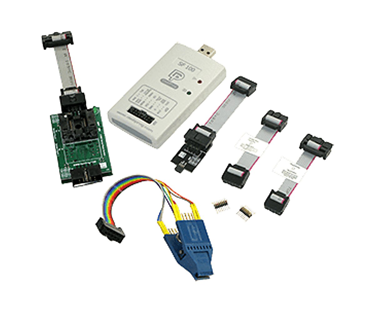
The SBK03 lets a board that uses an SO16W (300mil) SPI flash boot from a backup chip instead of the soldered one. The backup sits in DediProg’s BBF-16W Backup Boot Flash module. When it is connected, the onboard flash is disabled automatically, with no need to remove it. The module is transparent to the application, and most boards need no hardware change.
The SF100 programmer in the kit writes new images to the backup flash, so you can try a new build or go back to a known-good one without touching a soldering iron. The kit is also often used to boot a PC or board whose BIOS update failed, and then repair the corrupted BIOS with the usual flash utility tools.
Highlights
Serial flash emulator, transparent to the application
Disables the onboard serial flash automatically, with no need to remove it
No hardware change needed on most boards
Image download at 1Mbit/s, read at 2Mbit/s
USB interface with signal conflict protection
Two Ways to Connect
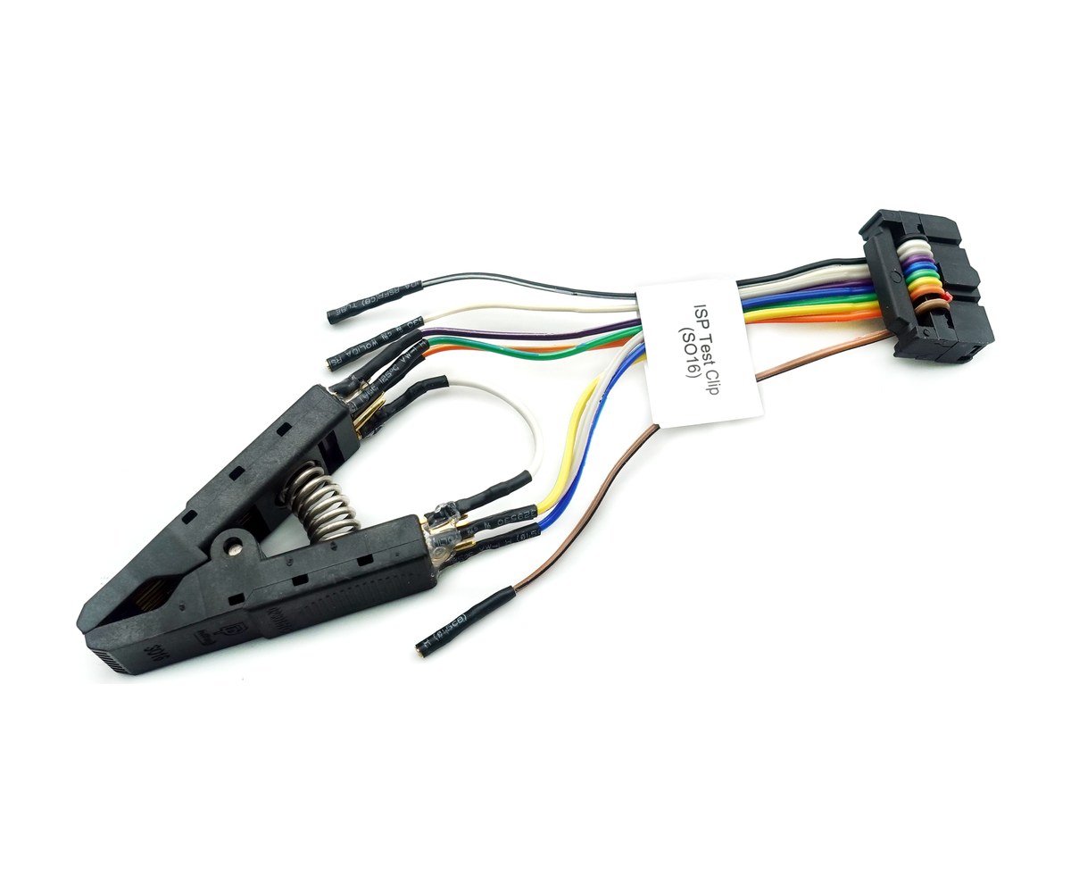
The SO16W test clip on the soldered flash
A 2.54mm 2×5 BBF connector, if the board was designed with one
Typical Uses
Booting a failing PC or board and repairing a corrupted BIOS
Trying new firmware builds without reflashing the soldered chip
Key Specifications
Spec
Value
Backup flash module
BBF-16W, SO16W (300mil) socket
Programmer
SF100, USB
Supported ICs
3.3V and 2.5V only
Speed
1Mbit/s download, 2Mbit/s read
Connection
SO16W test clip, or 2.54mm 2×5 BBF connector
Board requirement
Pull-up resistor between the HOLD pin and Vcc when the onboard flash stays on the board
For offline programming only, a socket adaptor is the better choice than a BBF kit.
In the Box
SF100 programmer with USB cable and SF100 ISP cable (ISP1-CB)
Universal adaptor (ISP-UADP-127) with BBF cable and 1.27mm 2×4 cable
CD-ROM with software, specifications and user manual
BBF-16W module with SO16W socket
SO16 connection adaptor (BBF-CON-16) with two 1.27mm 2×8 SMT headers
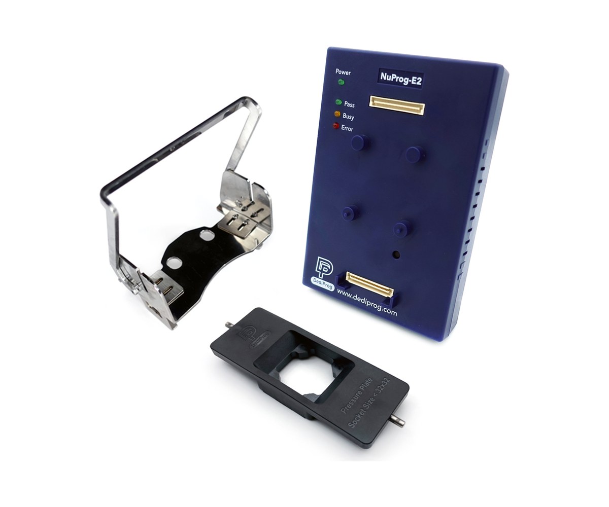
The NuProg-E2 Manual Kit puts DediProg’s NuProg-E2 engineering universal programmer together with the hand press fixture made for it and the DP socket press plate the fixture needs. With the fixture, one finger opens the socket, so changing parts at the bench is quick and easy on the hands.
The NuProg-E2 programs most IC types on the market: UFS, eMMC, MCU, CPLD, FPGA, SPI NOR and SPI NAND, parallel NOR and NAND, and EEPROM. It is built on an FPGA kernel and connects over SuperSpeed USB 3.0. It replaced the StarProg-U, which DediProg moved to end of life on 11 April 2023.
Highlights
FPGA kernel architecture for high-speed programming
UFS v2.0 to v4.0: descriptors, attributes and flags, plus LUN configuration
eMMC: user area, Boot1/2, extended CSD, RPMB, GPP1-4 and enhanced mode
Packages including CSP, BGA, QFN, QFP, SOP, TSOP, SSOP, PLCC and DIP
Projects and socket adaptors are shared with the NuProgPlus series
Hand press fixture opens a single 5kg socket adaptor with a 1:5 force ratio
Good to Know
The NuProg-E2 uses only the upper socket of a NuProgPlus dual socket adaptor
Socket adaptors for the older NuProg-E do not fit the NuProg-E2
In-system (on-board) programming is not available on the NuProg-E2
Engineering mode gives access to advanced features for development and repair work
Key Specifications
Spec
Value
Programmer
NuProg-E2 engineering universal programmer
Supported ICs
UFS, eMMC, MCU, CPLD, FPGA, SPI NOR, SPI NAND, parallel NOR and NAND, EEPROM
Packages
CSP, BGA, QFN, QFP, SOP, TSOP, SSOP, PLCC, DIP and more
File formats
Binary, Intel Hex, Motorola S19, and MCU-specific formats
Host interface
SuperSpeed USB 3.0; USB 2.0 with the power adapter connected
Operating system
Windows 7, 8, 8.1, 10, 11
Replaces
StarProg-U (end of life 11 April 2023)
In the Box
NuProg-E2 programmer with USB 3.0 cable, 5V/1A power supply and DP socket press plate
An additional DP socket press plate
Hand press fixture for NuProg-E2 (HPF-NuProg-E2)
Socket adaptors are ordered separately for each IC package. Tell us the part number and we will match the adaptor.
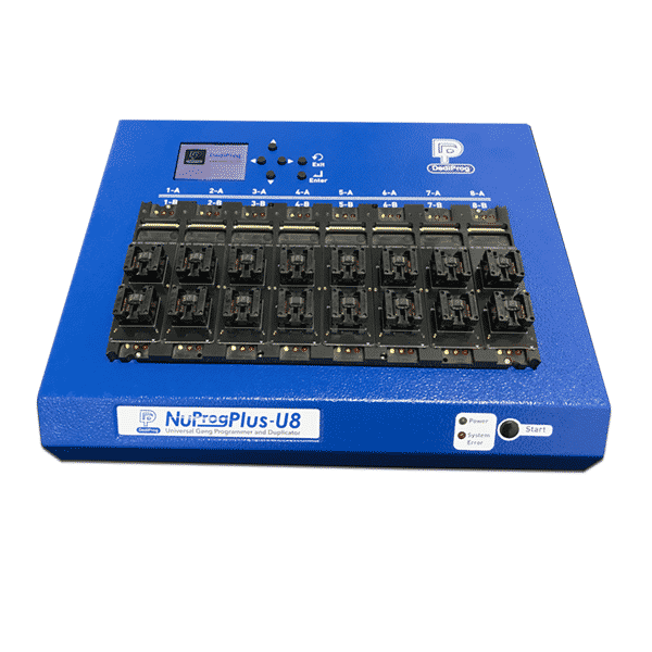
NuProgPlus-U8 Universal Gang Programmer and Duplicator (8 Sites)
Replaces the ProgMaster-U8, C8 and S8
The NuProgPlus-U8 programs up to 8 chips at the same time and runs on its own. Load a project file, then work from the LCD and keypad with no PC on the line. The operator only presses Start, so nobody can pick the wrong image file or part number by mistake.
It is the manual-operation model of DediProg’s NuProgPlus series, built on a newly designed FPGA kernel. It programs EEPROM, flash, MCU, eMMC and UFS devices and duplicates eMMC and UFS parts from a master device. It replaced the ProgMaster-U8, C8 and S8, which DediProg moved to end of life in September 2024.
Highlights
Up to 8 programming sockets, operated manually
Copy mode and Program mode
UFS, eMMC, SPI NOR, SPI NAND, parallel NOR and NAND, EEPROM, MCU, CPLD and FPGA
Built-in SSD for project files, with project download up to 100 MB/s
Three start modes: Manual, Auto Detection and Handler
A PC can link several NuProgPlus-U8 units and program on all of them at once
Duplication
UFS: data, LUN configuration, and descriptors, attributes and flags
eMMC: boot area, GPP, user area and ExtCSD
A master device is needed as the data source; RPMB is not duplicated
Production Features
NAND flash skip-bad-block management and partition files (CSV, DEF, MBN)
Project files lock the image and part number for each run
Packages including CSP, BGA, QFN, QFP, SOP, TSOP, SSOP, PLCC and DIP
Key Specifications
Spec
Value
Programming sites
Up to 8, manual operation
Operation
Stand-alone with LCD and keypad, or linked to a PC
Supported ICs
UFS, eMMC, SPI NOR, SPI NAND, parallel NOR and NAND, EEPROM, MCU, CPLD, FPGA
File formats
Binary, Intel Hex, Motorola S19, and MCU-specific formats
Storage
256GB SSD inside, upgradable to 512GB or 1TB
Project download
Up to 100 MB/s
Host interface
USB 3.0
Replaces
ProgMaster-U8, ProgMaster-C8, ProgMaster-S8 (end of life September 2024)
In the Box
NuProgPlus-U8 programmer
USB 3.0 cable
Power adaptor
256GB SSD, installed
Options: socket adaptors for your IC packages, an SSD upgrade to 512GB or 1TB, and the HPF-NuProgPlus-U8 hand press fixture, which opens all 8 single sockets at once.
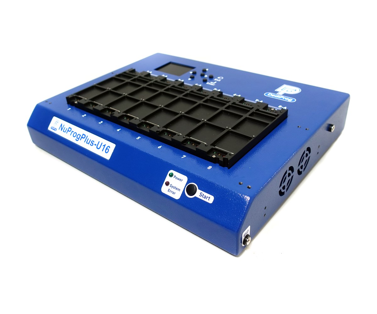
NuProgPlus-U16 Universal Gang Programmer and Duplicator
Up to 16 sites for SPI flash, eMMC and UFS
The NuProgPlus-U16 is the larger manual-operation model of DediProg’s NuProgPlus series. It comes with 8 programming sockets and can be extended to 16 sites, so it programs 16 SPI flash devices or duplicates 16 eMMC or UFS parts in parallel.
Like the rest of the series, it is built on a newly designed FPGA kernel and runs on its own: load a project file, then work from the LCD and keypad with no PC on the line. The operator only presses Start, so nobody can pick the wrong image file or part number by mistake. It programs EEPROM, flash, MCU, eMMC and UFS devices, and duplicates eMMC and UFS parts from a master device.
Highlights
8 programming sockets, expandable to 16 for SPI flash, UFS and eMMC
Copy mode and Program mode
UFS, eMMC, SPI NOR, SPI NAND, parallel NOR and NAND, EEPROM, MCU, CPLD and FPGA
Built-in SSD for project files, with project download up to 100 MB/s
Three start modes: Manual, Auto Detection and Handler
A PC can link several NuProgPlus-U16 units and program on all of them at once
Duplication
UFS: data, LUN configuration, and descriptors, attributes and flags
eMMC: boot area, GPP, user area and ExtCSD
A master device is needed as the data source; RPMB is not duplicated
Production Features
NAND flash skip-bad-block management and partition files (CSV, DEF, MBN)
Project files lock the image and part number for each run
Packages including CSP, BGA, QFN, QFP, SOP, TSOP, SSOP, PLCC and DIP
Key Specifications
Spec
Value
Programming sites
8 sockets, expandable to 16 for SPI flash, UFS and eMMC
Operation
Stand-alone with LCD and keypad, or linked to a PC
Supported ICs
UFS, eMMC, SPI NOR, SPI NAND, parallel NOR and NAND, EEPROM, MCU, CPLD, FPGA
File formats
Binary, Intel Hex, Motorola S19, and MCU-specific formats
Storage
256GB SSD inside, upgradable to 512GB
Project download
Up to 100 MB/s
Host interface
USB 3.0
In the Box
NuProgPlus-U16 programmer
USB 3.0 cable
Power adaptor
256GB SSD, installed
Options: socket adaptors for your IC packages, an SSD upgrade to 512GB, and the HPF-NuProgPlus hand press fixture, which opens 8 single or dual sockets at once.
The NuProg-E2 is DediProg’s universal engineering programmer. It programs most IC types on the market, including UFS, eMMC, MCU, CPLD, FPGA, SPI NOR and SPI NAND, parallel NOR and NAND, and EEPROM, in packages from CSP and BGA to QFN, QFP, SOP, TSOP, SSOP, PLCC and DIP.
It is built on an FPGA kernel for high programming speed and connects over SuperSpeed USB 3.0, so you can stay focused on development and application analysis. Its projects and socket adaptors are shared with the NuProgPlus production programmers, so work moves from the lab to the line without redoing it. It replaced the StarProg-U, which DediProg moved to end of life on 11 April 2023.
Highlights
FPGA kernel architecture for high-speed programming
UFS v2.0 to v4.0: descriptors, attributes and flags, plus LUN configuration
eMMC: user area, Boot1/2, extended CSD, RPMB, GPP1-4 and enhanced mode
Binary, Intel Hex, Motorola S19 and MCU-specific file formats
Projects and socket adaptors are shared with the NuProgPlus series
Regular software updates
Good to Know
The NuProg-E2 uses only the upper socket of a NuProgPlus dual socket adaptor
Socket adaptors for the older NuProg-E do not fit the NuProg-E2
In-system (on-board) programming is not available on the NuProg-E2
For a stable connection, plug in the power adapter first, then the USB cable
Engineering mode gives access to advanced features for development and repair work
Key Specifications
Spec
Value
Programmer
Single-site engineering universal programmer
Supported ICs
UFS, eMMC, MCU, CPLD, FPGA, SPI NOR, SPI NAND, parallel NOR and NAND, EEPROM
Packages
CSP, BGA, QFN, QFP, SOP, TSOP, SSOP, PLCC, DIP and more
UFS
v2.0, v2.1, v3.0, v3.1, v4.0
eMMC
User area, Boot1/2, ExtCSD, RPMB, GPP1-4, enhanced mode
Host interface
SuperSpeed USB 3.0; USB 2.0 with the power adapter connected
Operating system
Windows 7, 8, 8.1, 10, 11
Replaces
StarProg-U (end of life 11 April 2023)
In the Box
NuProg-E2 programmer
USB 3.0 cable
5V/1A power supply (100-240V AC)
DP socket press plate
Socket adaptors are ordered separately for each IC package. Tell us the part number and we will match the adaptor.
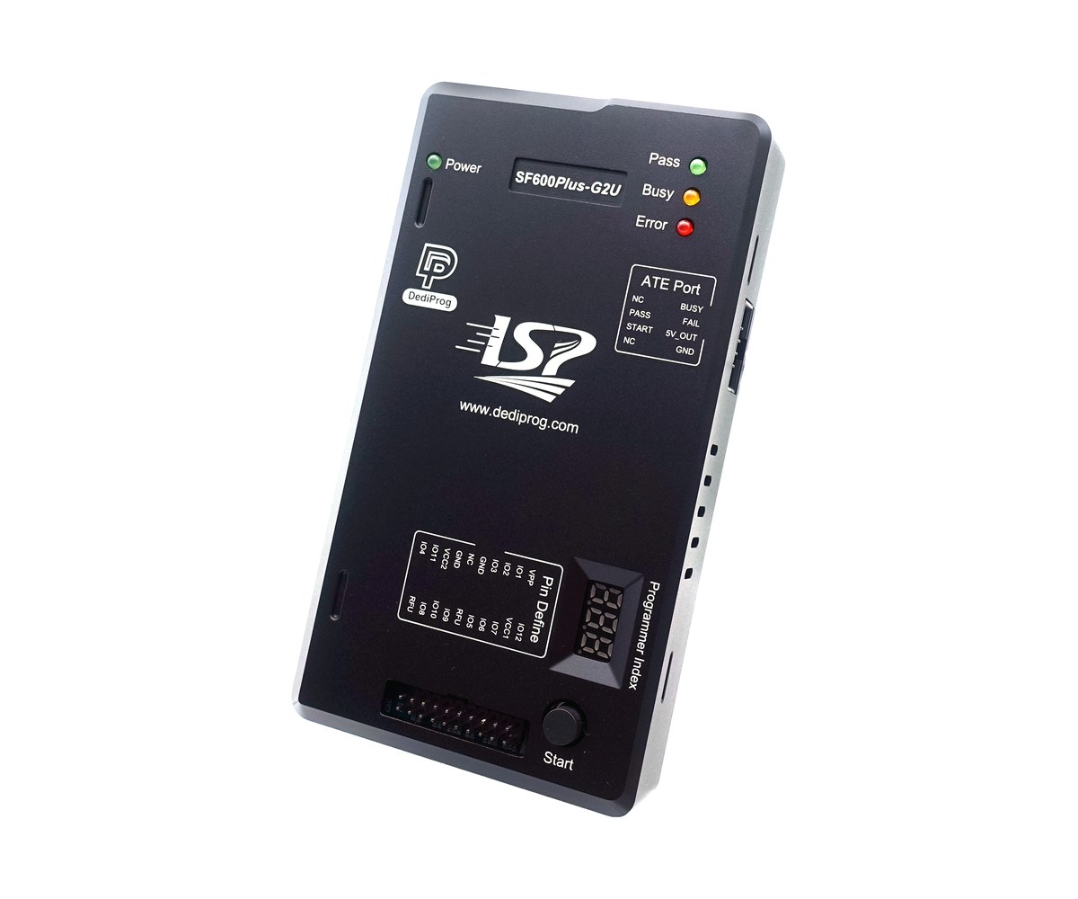
ISP and stand-alone universal programmer for production lines
The SF600Plus-G2U is a high-speed universal programmer for in-system (on-board) programming and for stand-alone programming. It programs MCU, FPGA, CPLD, SPI NOR and SPI NAND flash, and EEPROM, and it is controlled over USB or its ATE port, so it fits into in-line ICT and FCT test platforms on an EMS production line.
It is fully compatible with DediProg’s SF600Plus-G2 SPI flash programmer and adds a dedicated on-board programming application. It replaced the StarProg-A and the K110, which DediProg moved to end of life on 1 December 2022. DediProg supplies the SF600Plus-G2U only to customers who have ordered the device license, so contact Pertech to set it up.
Highlights
Protocols including SWD, JTAG, DAP, UART, I2C, CAN and LIN
Synchronous or asynchronous programming across several programmers and boards
Programming voltage from 1.2V up to 12V
Custom scripts for the programming sequence
Project mode for stand-alone work, with the ATE port for in-line control
ARM and FPGA architecture with 4GB of embedded memory
Software
DPISP CLI: for engineers debugging or verifying from the command line
DPISP GUI, Engineering mode: for programming ICs with finalized scripts
DPISP GUI, Production mode: for mass production, on-line or stand-alone
Blank check, erase, program, verify, and option register editing
Windows 8, 8.1, 10, 11
Key Specifications
Spec
Value
Architecture
ARM and FPGA
Embedded memory
4GB
PC connection
USB 2.0 Type-C, Ethernet
ATE interface
Start, Pass, Busy and Error control and status lines, 5V TTL
Programming
In-system (ISP); off-line mode with SPI socket adaptors only
Supported ICs
EEPROM, SPI NOR and NAND flash, MCU, FPGA, CPLD and more
The EM100Pro-G3 stands in for the SPI NOR flash on your board. You load a new firmware image into the emulator and the target boots from it at once, so there is no need to reprogram or desolder the flash chip after every build. DediProg developed it together with leading SPI NOR flash suppliers to cover both current and next-generation devices, from 512Kbit up to 4Gbit, in one tool.
It replaces the EM100Pro-G2, which DediProg moved to end of life on 5 July 2023. The G3 is built on an FPGA architecture, and on large images it updates code in half the time: a 1Gb image takes 10 seconds instead of 20 (erase, program and verify).
Highlights
Emulates SPI NOR flash devices from 512Kbit to 4Gbit, at 1.8V or 3.3V
Single, Dual and Quad IO, up to 50MHz in each mode
Up to twice as fast as the EM100Pro-G2 on 512Mb to 2Gb images
Display and edit the emulated memory content
Built-in SPI bus analyzer and SPI HyperTerminal, with a high-speed internal buffer for trace logs
Connects to Intel motherboards through an optional Intel ISP adaptor
USB 2.0 connection to the host PC
Key Specifications
Spec
Value
Emulated Capacity
512Kbit to 4Gbit SPI NOR Flash
Voltage Support
1.8V / 3.3V
IO Modes
Single / Dual / Quad IO, up to 50MHz
Code Update (erase, program, verify)
3s up to 256Mb; 5s at 512Mb; 10s at 1Gb; 20s at 2Gb
Target Connectors
2×10 header (emulation signals) and 2×2 header (reset and trigger), 2.54mm pitch
Host Interface
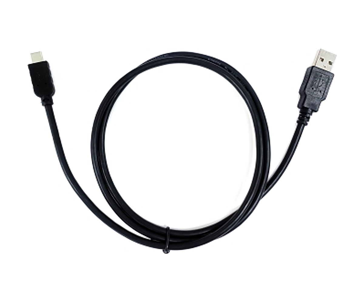
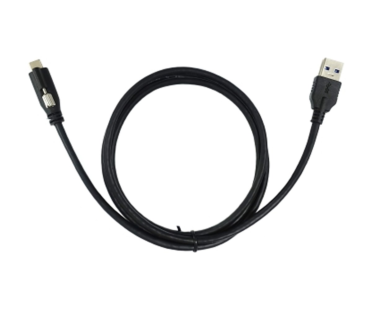
USB 2.0 (1m USB-A to USB-C cable included)
SPI Trace
Built-in SPI Bus Analyzer & HyperTerminal
Intel Platforms
Optional Intel ISP Adaptor-C or Adaptor-C2
Replaces
EM100Pro-G2 (end of life 5 July 2023)
In the Box
EM100Pro-G3 emulator and USB 2.0 cable (1m, USB-A to USB-C)
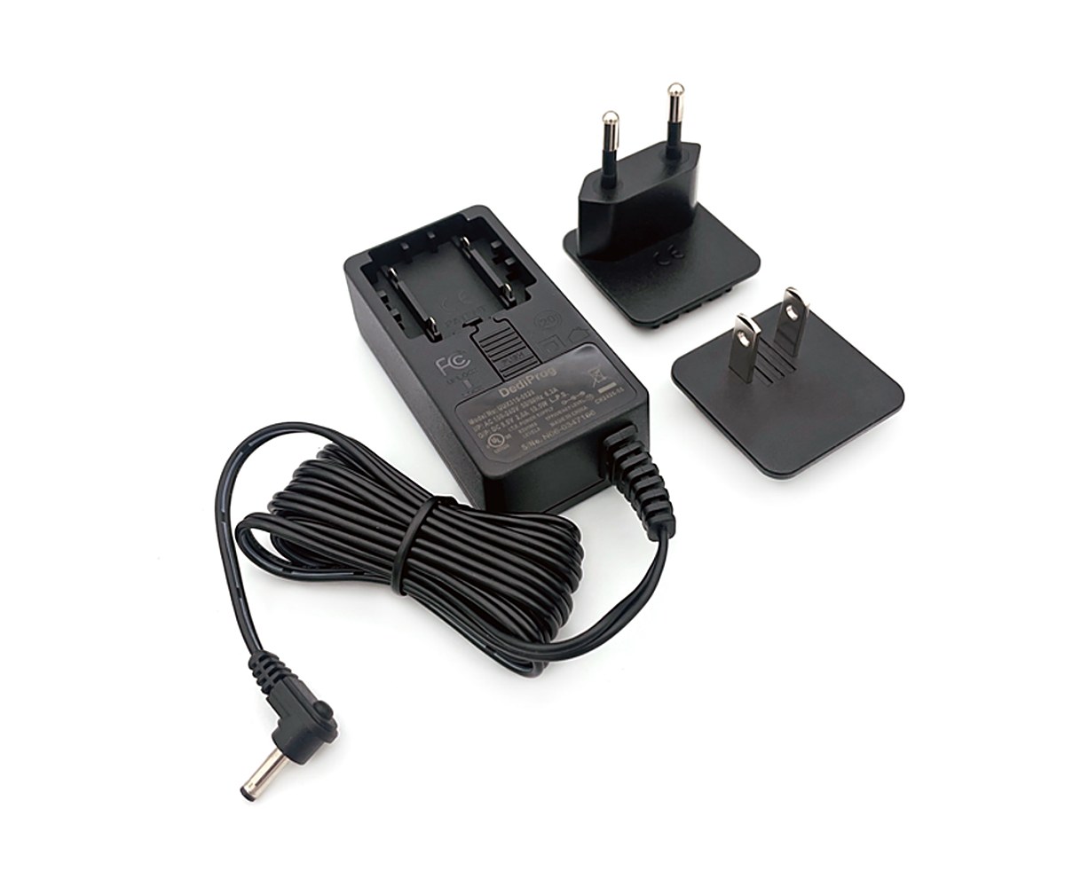
Power adapter with US and EU plugs
SO8W and SO16W reference flash adaptors
Connection cables, SMT headers and grabber clips
For the EM100Pro-G3 software, the user manual or a quote, contact Pertech.
SIGLENT’s SDS5000L series is a low-profile (1U), display-less digital storage oscilloscope module, available in bandwidths of 350 MHz, 500 MHz, and 1 GHz, with 8 analog channels + 1 external trigger. All models sample at up to 5 GSa/s and offer a maximum record length of 2.5 Gpts per channel.
The SDS5000L series employs Siglent’s SPO technology with a maximum waveform capture rate of up to 160,000 wfm/s in normal mode and 650,000 wfm/s in Sequence mode, 256-level intensity grading display, and a color temperature display mode. It supports advanced triggering including edge, pulse, pattern, and serial bus triggering for I2C, SPI, UART, CAN, and other protocols.
Designed without an integrated display for standalone rack use with an external monitor, or for multi-unit synchronization via the SYN64 distributor supporting up to 512 total channels. The unit features 1000 Mbps Ethernet connectivity and SCPI remote control support.
Bandwidth
Channels
Real time sampling rate
Capture rate
Memory depth
SDS5038L
350 MHz
8 + EXT
5 GSa/s
650,000 wfm/s
2.5 Gpts/ch
SDS5058L
500 MHz
8 + EXT
5 GSa/s
650,000 wfm/s
2.5 Gpts/ch
SDS5108L
1 GHz
8 + EXT
5 GSa/s
650,000 wfm/s
2.5 Gpts/ch
Key Features
8 analog channels + 1 external trigger, up to 1 GHz bandwidth with up to 5 GSa/s sample rate
12-bit ADC
SPO technology
Waveform capture rates up to 160,000 wfm/s in Normal mode and 650,000 wfm/s in Sequence mode
Supports 256-level intensity grading and color temperature display modes
Up to 2.5 Gpts/ch record length
Segmented acquisition (Sequence) mode, up to 170,000 segments
Automatic measurements on 60+ parameters
8 Math traces with FFT analysis
Low-profile (1U) module without integrated display, designed for external monitor use or SYN64 multi-unit synchronization (up to 512 total channels)
1000 Mbps Ethernet connectivity, SCPI remote control support
SIGLENT’s SDS5000X HD series digital storage oscilloscopes are 12-bit high resolution instruments available in bandwidths of 350 MHz, 500 MHz, and 1 GHz, with 4, 6, or 8 analog channels + 16 digital channels for mixed-signal analysis. All models sample at up to 5 GSa/s and offer a maximum record length of 2.5 Gpts per channel.
The SDS5000X HD series employs Siglent’s SPO technology with a maximum waveform capture rate of up to 160,000 wfm/s in normal mode and 650,000 wfm/s in Sequence mode, 256-level intensity grading display, and a color temperature display mode. A low-noise front end delivers a typical noise floor as low as 140 µVrms at 1 GHz bandwidth, with a typical ENOB of 8.2 bits at 1 GHz. The trigger system supports advanced serial bus triggering and decoding for I2C, SPI, UART, CAN, LIN, and other protocols.
The large 12.1″ capacitive touchscreen display (1280 × 800) supports multi-touch gestures, with mouse control and remote web control over LAN also supported.
Bandwidth
Channels
Real time sampling rate
Capture rate
Memory depth
SDS5034X HD
350 MHz
4 + EXT
5 GSa/s
650,000 wfm/s
2.5 Gpts/ch
SDS5054X HD
500 MHz
4 + EXT
5 GSa/s
650,000 wfm/s
2.5 Gpts/ch
SDS5104X HD
1 GHz
4 + EXT
5 GSa/s
650,000 wfm/s
2.5 Gpts/ch
SDS5036X HD
350 MHz
6 + EXT
5 GSa/s
650,000 wfm/s
2.5 Gpts/ch
SDS5056X HD
500 MHz
6 + EXT
5 GSa/s
650,000 wfm/s
2.5 Gpts/ch
SDS5106X HD
1 GHz
6 + EXT
5 GSa/s
650,000 wfm/s
2.5 Gpts/ch
SDS5038X HD
350 MHz
8 + EXT
5 GSa/s
650,000 wfm/s
2.5 Gpts/ch
SDS5058X HD
500 MHz
8 + EXT
5 GSa/s
650,000 wfm/s
2.5 Gpts/ch
SDS5108X HD
1 GHz
8 + EXT
5 GSa/s
650,000 wfm/s
2.5 Gpts/ch
Key Features
4, 6, or 8 analog channels, up to 1 GHz bandwidth with up to 5 GSa/s sample rate
SIGLENT’s SDS6000L series Low Profile Digital Storage Oscilloscopes provide up to 8 analog channels + 16 digital channels in a space-saving chassis size. This series is available in bandwidths of 2 GHz / 1 GHz / 500 MHz, features a maximum sample rate of 5 GSa/s (10 GSa/s ESR) for each channel, and a maximum record length of 500 Mpts/ch.
The SDS6000L series employs Siglent’s SPO technology with a maximum waveform capture rate of up to 170,000 wfm/s (normal mode, up to 750,000 wfm/s in Sequence mode), 256-level intensity grading display function plus a color temperature display mode. It also employs an innovative digital trigger system with high sensitivity and low jitter. The trigger system supports multiple powerful triggering modes, including serial bus triggering. Tools such as History waveform recording, Search and Navigate functions, Mask Test, Power Analysis, and Eye/Jitter Analysis allow extended waveform records to be captured, stored, and analyzed. An impressive array of measurement and math capabilities, options for a 25 MHz arbitrary waveform generator, and serial decoding are also features of the SDS6000L.
It can be used as a stand-alone oscilloscope by being connected to an external display and a mouse. It can also be remotely controlled over LAN thanks to the convenient built-in web server. Combined with a 64-channel synchronization distributor (SYN64), multiple SDS6000L modules can be organized as a high-speed acquisition system with up to 512 channels. A complete SCPI command set over the standard 1000M LAN connection provides very fast data acquisition to speed automated test applications.
Waveform capture rates up to 170,000 wfm/s (normal mode), and 750,000 wfm/s (sequence mode)
Supports 256-level intensity grading and color temperature display modes
500 Mpts Record length in total for all 4 channels
Digital trigger system
Intelligent trigger: Edge, Slope, Pulse, Window, Runt, Interval, Dropout, Pattern, Qualified, Nth edge, Setup/hold, Delay and Video (HDTV supported). Zone Trigger simplifies advanced triggering
Serial bus triggering and decoder, supports protocols I2C, SPI, UART, CAN, LIN, CAN FD, FlexRay, I2S, MIL-STD-1553B, SENT and Manchester
Segmented acquisition (Sequence) mode, dividing the maximum record length into multiple segments (up to 80,000), according to trigger conditions set by the user, with a very small dead time between segments to capture the qualifying event
History waveform record (History) function, the maximum recorded waveform length is 80,000 frames
Automatic measurements on 50+ parameters, supports statistics with histogram, track, trend, Gating measurement, and measurements on Math, History, Memory and Ref
4 Math traces (8 Mpts FFT, addition, subtraction, multiplication, division, integration, differential, square root, etc.), supports formula editor
Abundant data analysis functions such as Search, Navigate, Digital Voltmeter, Counter, Waveform Histogram, Power Analysis and Eye/Jitter Analysis
Interfaces include: 4x USB Hosts, USB Device (USBTMC), 1000M LAN (VXI-11/Telnet/Socket), micro SD card, Pass/Fail, Trigger Out, HDMI, 10MHz In, 10MHz Out
Built-in web server supports remote control over the LAN port using a web browser. Supports SCPI remote control commands. Supports external mouse and keyboard.
SIGLENT’s SDS1000X HD series high resolution digital storage oscilloscopes are based on 2 GSa/s, 12-bit Analog-Digital Converters and front ends with excellent noise floor performance. They are available in bandwidths of 200 MHz and 100 MHz, have maximum record length of 100 Mpts, and display 2/4 analog channels + 16 digital channels mixed signal analysis ability.
The SDS1000X HD series employs Siglent’s SPO technology with a maximum waveform capture rate of up to 120,000 wfm/s (normal mode, up to 500,000 wfm/s in Sequence mode), 256-level intensity grading display function plus a color temperature display mode. It also employs an innovative digital trigger system with high sensitivity and low jitter. The trigger system supports multiple powerful triggering modes including serial bus triggering. Tools such as History waveform recording, Search and Navigate functions, Mask Test, Bode Plot, Power Analysis allow for extended waveform records to be captured, stored, and analyzed. An impressive array of measurement and math capabilities, options for a 25 MHz arbitrary waveform generator, as well as serial decoding are also features of the SDS1000X HD.
The large 10.1″ display capacitive touch screen supports multi-touch gestures, with the addition of user-friendly UI design, can greatly improve the operation efficiency. It also supports mouse control, and remote web control over LAN.
Bandwidth
Channels
Real time sampling rate
Capture rate
Memory depth
SDS1102X HD
100 MHz
2 + EXT
2 GSa/s
500,000 wfm/s
100 Mpts/ch
SDS1104X HD
100 MHz
4 + EXT
2 GSa/s
500,000 wfm/s
100 Mpts/ch
SDS1202X HD
200 MHz
2 + EXT
2 GSa/s
500,000 wfm/s
100 Mpts/ch
SDS1204X HD
200 MHz
4 + EXT
2 GSa/s
500,000 wfm/s
100 Mpts/ch
Key Features
12-bit Analog-Digital Convertors with sample rate up to 2 GSa/s
Front ends with 70 μVrms noise floor @ 200 MHz bandwidth
2/4 analog channels, up to 200 MHz bandwidth
SPO technology
Waveform capture rate up to 120,000 wfm/s (normal mode), and 500,000 wfm/s (sequence mode)
Supports 256-level intensity grading and color temperature display modes
Up to 100 Mpts record length
Digital trigger system
Intelligent trigger: Edge, Slope, Pulse width, Window, Runt, Interval, Dropout, Pattern, Video (HDTV supported), Qualified, Nth edge, Delay, Setup/Hold time
Serial bus triggering and decoder, supports protocols I2C, SPI, UART, CAN, LIN, CAN FD (decode only), FlexRay (decode only)
Segmented acquisition (Sequence) mode, dividing the maximum record length into multiple segments (up to 80,000), according to trigger conditions set by the user, with a very small dead time between segments to capture the qualifying event
History waveform record (History) function, the maximum recorded waveform length is 80,000 frames
Automatic measurements on 50+ parameters, supports statistics with histogram, track, trend, Gating measurement, and measurements on Math, History and Ref
4 Math traces (2 Mpts FFT, addition, subtraction, multiplication, division, integration, differential, square root, etc.), supports formula editor
Abundant data analysis functions such as Search, Navigate, Counter, Bode plot and Power Analysis
High Speed hardware-based Mask Test function, with Mask Editor tool for creating user-defined masks
16 digital channels
25 MHz waveform generator (optional)
Large 10.1″ TFT-LCD display with 1024 x 600 resolution; Capacitive touch screen supports multi-touch gestures
Interfaces include: USB Hosts, USB Device (USBTMC), LAN (VXI-11/Telnet/Socket), Pass/Fail, Trigger Out
Built-in web server supports remote control over the LAN port using a web browser. Supports SCPI remote control commands. Supports external mouse and keyboard.
SIGLENT’s SDS800X HD series high resolution digital storage oscilloscopes are based on 2 GSa/s, 12-bit Analog-Digital Converters and front ends with excellent noise floor performance. They are available in bandwidths of 200 MHz, 100 MHz and 70 MHz, have maximum record length of 100 Mpts, and display 2/4 analog channels + 16 digital channels mixed signal analysis ability.
The SDS800X HD series employs Siglent’s SPO technology with a maximum waveform capture rate of up to 120,000 wfm/s (normal mode, up to 500,000 wfm/s in Sequence mode), 256-level intensity grading display function plus a color temperature display mode. It also employs an innovative digital trigger system with high sensitivity and low jitter. The trigger system supports multiple powerful triggering modes including serial bus triggering. Tools such as History waveform recording, Search and Navigate functions, Mask Test, Bode Plot, Power Analysis allow for extended waveform records to be captured, stored, and analyzed. An impressive array of measurement and math capabilities, options for a 25 MHz arbitrary waveform generator, as well as serial decoding are also features of the SDS800X HD.
The 7″ display capacitive touch screen supports multi-touch gestures, with the addition of user-friendly UI design, can greatly improve the operation efficiency. It also supports mouse control, and remote web control over LAN.
Bandwidth
Channels
Real time sampling rate
Capture rate
Memory depth
SDS802X HD
70 MHz
2
2 GSa/s
500,000 wfm/s
50 Mpts/ch
SDS804X HD
70 MHz
4
2 GSa/s
500,000 wfm/s
50 Mpts/ch
SDS812X HD
100 MHz
2
2 GSa/s
500,000 wfm/s
50 Mpts/ch
SDS814X HD
100 MHz
4
2 GSa/s
500,000 wfm/s
50 Mpts/ch
SDS822X HD
200 MHz
2
2 GSa/s
500,000 wfm/s
100 Mpts/ch
SDS824X HD
200 MHz
4
2 GSa/s
500,000 wfm/s
100 Mpts/ch
Key Features
12-bit Analog-Digital Convertors with sample rate up to 2 GSa/s
Front ends with 70 μVrms noise floor @ 200 MHz bandwidth
2/4 analog channels, up to 200 MHz bandwidth
SPO technology
Waveform capture rate up to 120,000 wfm/s (normal mode), and 500,000 wfm/s (sequence mode)
Supports 256-level intensity grading and color temperature display modes
Up to 100 Mpts record length
Digital trigger system
Intelligent trigger: Edge, Slope, Pulse width, Window, Runt, Interval, Dropout, Pattern, Video (HDTV supported), Qualified, Nth edge, Delay, Setup/Hold time
Serial bus triggering and decoder, supports protocols I2C, SPI, UART, CAN, LIN
Segmented acquisition (Sequence) mode, dividing the maximum record length into multiple segments (up to 80,000), according to trigger conditions set by the user, with a very small dead time between segments to capture the qualifying event
History waveform record (History) function, the maximum recorded waveform length is 80,000 frames
Automatic measurements on 50+ parameters, supports statistics with histogram, track, trend, Gating measurement, and measurements on Math, History and Ref
4 Math traces (2 Mpts FFT, addition, subtraction, multiplication, division, integration, differential, square root, etc.), supports formula editor
Abundant data analysis functions such as Search, Navigate, Counter, Bode plot and Power Analysis
High Speed hardware-based Mask Test function, with Mask Editor tool for creating user-defined masks
16 digital channels
25 MHz waveform generator (optional)
7″ TFT-LCD display with 1024 x 600 resolution; Capacitive touch screen supports multi-touch gestures
Interfaces include: USB Hosts, USB Device (USBTMC), LAN (VXI-11/Telnet/Socket), Pass/Fail, Trigger Out
Built-in web server supports remote control over the LAN port using a web browser. Supports SCPI remote control commands. Supports external mouse and keyboard. Supports NTP.